Ben Eater 8-bit computer project
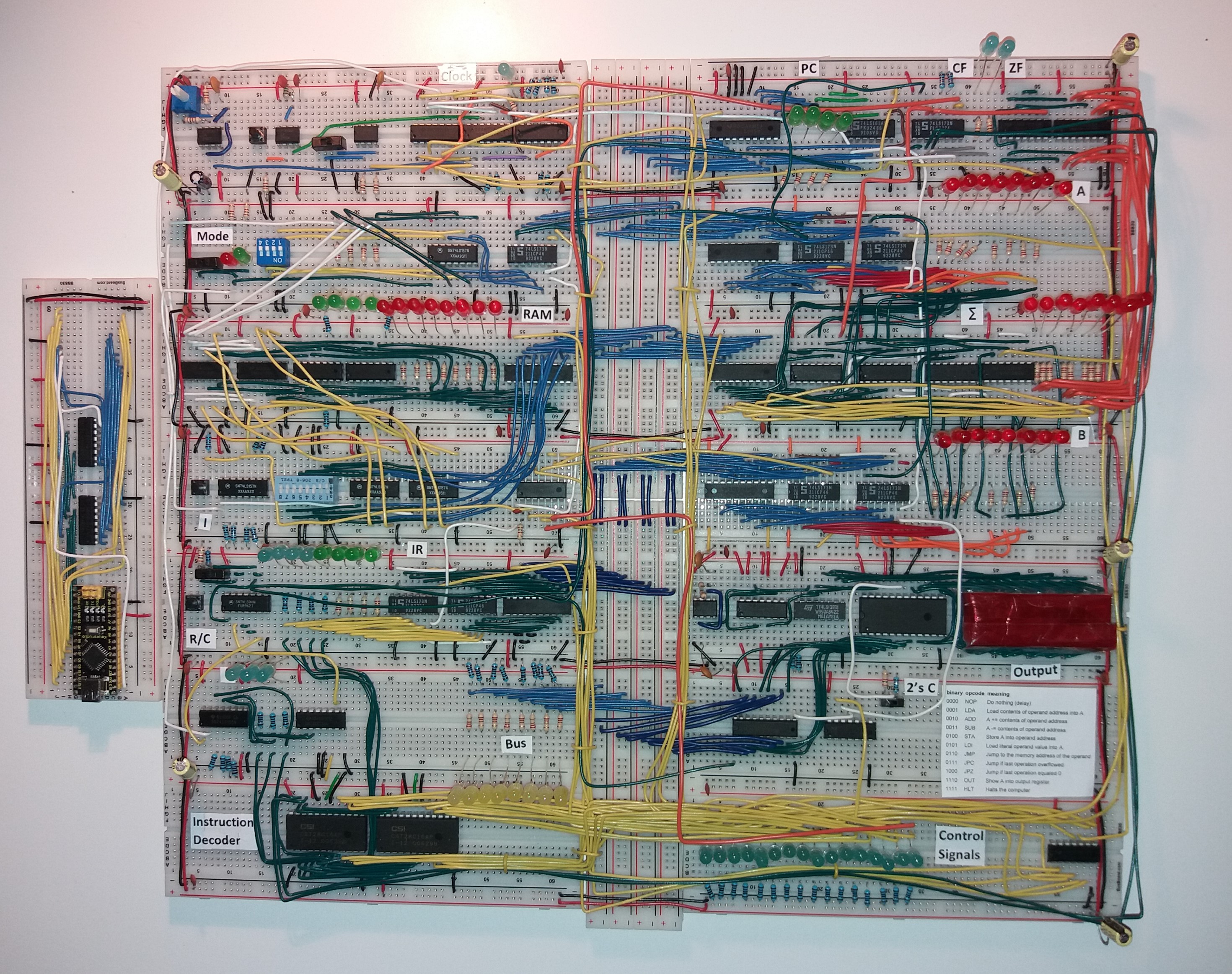
Table of Contents
- Table of Contents
- Introduction
- Clock
- Registers
- Arithmetic Logic Unit (ALU)
- Random Access Memory (RAM)
- Register recap
- Difference between registers and memory
- Address decoder
- 74LS189 (16 4-word address RAM)
- Building the RAM
- Building the memory address register (and a “programming mode” version)
- Building an 8-bit input terminal for the RAM (to manually store a program) and the alternative of inputs from the Bus
- Testing the RAM
- Labeling jumperwires (control signals) and architecture overview
- Program counter (PC)
- Output module
- Terminology review
- Control unit
- Last minute fixes
- Programs
Introduction
Ben Eater is an online educator on computer-related topics from which I’m following his 8-bit computer project. https://eater.net/8bit. The computer is composed of different modules, which are built on breadboards. The modules are the clock module, registers and ALU (arithmetic and logic unit) module, RAM (random access memory) and program counter module, and output and control logic module.
- To refresh circuit analysis basics check this post.
- You can also check my CSE1400 Computer Organization notes
Computer features
- Specsheet
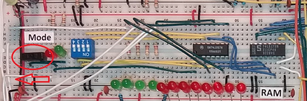
- How to operate:
- Set clock to monostable by moving the slideswitch to the right (manual clock pulse)
- Set mode to programming mode with the slide switch (left = red led on = programming mode)
- Use the 4-bit DIP switches to change the address of the RAM
- Use the 8-bit DIP switches to set the contents of the RAM and press the Input button (I) to save them
- Reset all registers and counters with the R/C button with the “clear” switch on (to the right)
- Set the computer back to run mode (slide switch to right = green led on = run mode), and set the clock to astable by moving the slideswitch to the left and adjust the speed with the potentiometer
- Set clock to monostable by moving the slideswitch to the right (manual clock pulse)
- Use this assembly language for your programs, this compiler to turn it into binary and you may as well use this forked repo to simulate the program execution
- Fibonacci demo:
- The computer is “turing complete” because it allows the execution of a program and the computer supports addition, subtraction and conditional jumps, from which any computable problem, given infinite memory, could be computed.
Power supply
We will be using a 5V (volt) power source, which Ben has crafted by cutting off the wires of a cellphone charger.
- Safety rules before using anything related to electricity:
- Dont plug a lot of stuff into a single extension cord
- Keep eletrcical things far away from water
- Never connect LEDs directly to 5 volt source without a current limiting resistor or you will damage the LED.
- Most 74LSxx logic chips have internal resistors that let you connect LEDS directly to the outputs without a resistor. However, the 555 timer, 74189 RAM, 28C16 EEPROM and 74HC595 do not.
- For most reliable results you may want to connect a \(220\Omega\) resistor in series with every LED.
Breadboards
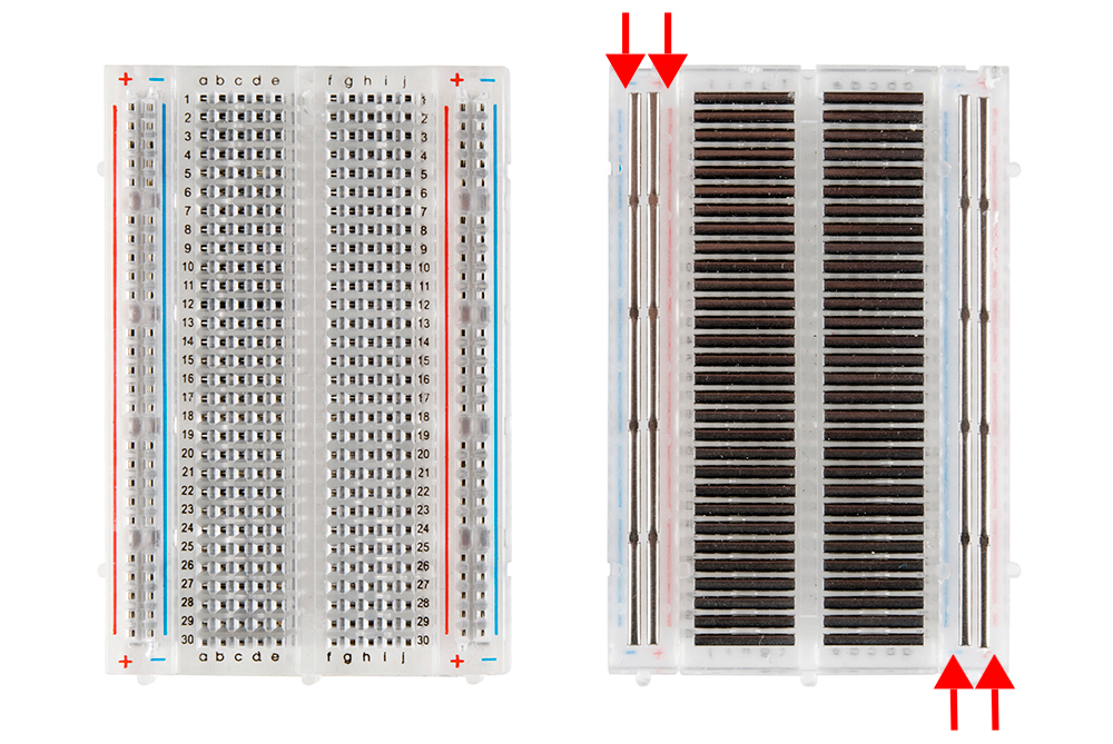
- The breadboard is composed of metalical strips that can be linked together with jump wires and electrical components.
- The A-J holes constitute columns (each) and the numbers constitute rows.
- A1, B1, C1, D1 and E1 are all connected, and not connected to any other wholes in the breadboard.
- The individual power buses are not connected to each other (only the column itself).
- The + - vertical strips are called buses or rails and are used to deliver power.
- The red (+) line will connect to the positive terminal of the battery
- The black or blue (-) line will connect to the negative terminal of the battery
- The busline may not connect the entire length of the board, unbroken lines show that the bus indeed connects the entire length
- The middle space of the breadboard is designed to fit the integrated circuits (IC) (chips) that come with dual in-line package (DIP), meaning they come in two columns of pins of which each individual pin is connected to its own row.
Sample closed circuit
- The long leg is the positive side of the LED and it’s called anode, and the shorter leg is for the negative side and it’s called cathode.
- Plugging it backwards wont break the led, but it will block the current flow of the circuit.
Common mistakes
- Setting the LD legs in different rows
- Loose wires not pushed deep into the wholes
- Disrespecting the polarity of the components
- LEDs have polarity: long leg +, short leg -
- Resistors don’t have polarity
- Jumper wires:
- Long flexible wires are convinient for simple circuits but will spagetti-like mess up complex circuits
- Pre-cut wires have predefined lengths which limit customization
- hookup wire and wire strippers to make your own wires:
- Make sure to buy solid-core wire and not stranded wire as the latter is made up of multiple individual strands which makes the ends much harder to push into a breadboard
- As a last resort if stranded wired cannot be solded it can be twisted to increase its tightness.
- To leave enough space for bending the wires and plug them into the board leave a room of 3 more wholes.
- Integrated circuits:
- Not connecting an integrated circuit in the middle of the board as that will connect both ends of the IC (making a shortircuit)
Disclaimers
IC numbers and logic families
For example, let’s break down SN74LS161A.:
- SN - these prefixes typically just tell you what manufacturer it is. For example, SN is used by Texas Instruments. As far as I know, you can ignore this.
- 74 - denotes that it’s a standard consumer chip. There are a few other types, like military and automotive
- LS - this is the logic family. Do not mix chips from different logic families unless you know they are compatible (i.e. LS and HCT)
- LS - Low-power schottky. Built with transistor-transistor logic (TTL). What Ben uses. Old. Not really that low-power compared to newer chips. Pretty damned resilient. Not compatible with HC.
- HC - CMOS. Uses much less power. A bit less forgiving and not compatible with LS or other TTL chips.
- HCT - A special kind of CMOS designed to work with TTL chips.
- You may also find chips without a logic family (i.e. 74161). They are regular TTL chips.
- 161 - the actual chip number. This one is a synchronous 4-bit binary counter.
- A - this depends on the chip, but may denote the form factor - i.e. 40-pin DIP. Information may be in the datasheet.
Pulling resistors
- Pull-up and Pull-down resistors are used to correct bias the inputs of digital gates to stop them from having inpredctable high/low values when there is no input condition.
- If you tie a pin to VCC with a resistor, it’s said to be “pulling the pin up”, and if you tie it to GND it’s “pulling the pin down”, hence the terms pull-up and pull-down.
- Unused LS-series inputs should typically be tied in a way such that the corresponding output is always high. (this is to consume less power, the arch-rival of the project)
- Some of the push buttons also need resistors so that they aren’t “floating” when they’re disconnected. For example, I added a 1K pull-up to the RAM write button.
- Some chips families are less forgiving about floating inputs, so as a thumb rule you should never leave an input pin unconnected (floating).
- An open CMOS input pin is in a “high impedance” state, which means there won’t be any substantial opportunity for a charge built up on the pin to dissipate and the Voltage of the pin will drift around due to internal and external leakage.
- In TTL 74LS serie, a input signal between 0 and 0.8V is considered “LOW”, and a input signal between 2.0 and 5.0V is considered “HIGH”. Any voltage between 0.8 and 2.0 volts is undefined. Therefore, you have to guarantee in your design that you will never enter in the uncertainty zone.
- A Ben follower suggested to use 10k resistors, other suggested 1k, also for the Bus default pull-down resistors (instead of the 10k of Ben’s build). So use 10k for pull-up and 1k for pull-down.
- But there’s actually an accurate way to calculate them
- Connecting directly to VCC (or even ground) might be a bad idea because a high current will flow through the pull-up resistor, heating the device and using up an unnecessary amount of power when the switch is closed. So the idea is to calculate the MAX resistor value, and then round it down to the nearest standard commercial resistor value out there.
- A rule of thumb is to use a resistor that is at least 10 times smaller than the value of the input pin impedance. In bipolar logic families which operate at operating at 5V, the typical pull-up resistor value is 1-5 kΩ. For switch and resistive sensor applications, the typical pull-up resistor value is 1-10 kΩ. If in doubt, a good starting point when using a switch is 4.7 kΩ. Some digital circuits, such as CMOS families, have a small input leakage current, allowing much higher resistance values, from around 10kΩ up to 1MΩ. The disadvantage when using a larger resistance value is that the input pin responses to voltage changes slower.
Max Pull-up Resistor Value
\[Rmax = \frac{V_{CC}-V_{IH(MIN)}}{I_{IH(MAX)}}\]where: \(V_{IH(MIN)}\) is the minimum input voltage guaranteed to be recognized as a logic “1” (2V approx., but see in datasheet). \(I_{IH(MAX)}\) is the max current flows into the TTL input when the input is a ‘HIGH’ (see in datasheet).
If you use a higher resistor, you will have a voltage within the undefined zone.
For the pull-down resistor, the analysis is similar.
Max Pull-down Resistor Value
\[Rmax = \frac{V_{IL(MAX)}-V_{IL(MIN)}}{I_{IL(MAX)}}\]where: \(V_{IL(MAX)}\) is the maximum input voltage guaranteed to be recognized as a logic ‘0’.(0.8V approx., but see in datasheet). where: \(V_{IL(MIN)}\) is the minimum input voltage guaranteed to be recognized as a logic ‘0’. (0V approx., but see in datasheet). \(I_{IL(MAX)}\) is the max current flows into the TTL input when the input is a ‘LOW’ (see datasheet).
Again, if you use a higher resistor, you will have a voltage within the undefined zone.
Power
- The LS series chips are designed to run with no less than 4.75 volts. That gives you very little wiggle room. You absolutely need to have good power distribution.
- Run “main” power rails down both sides of the computer and connect every regular power rail on your computer directly to the main power rails. This will eliminate the daisy-chaining completely and ensure (nearly) optimal power distribution.
- Alternatively connect power rails from left side of the Bus breadboards with right side of the Bus breadboards, at least once for each breadboard.
- Run “main” power rails down both sides of the computer and connect every regular power rail on your computer directly to the main power rails. This will eliminate the daisy-chaining completely and ensure (nearly) optimal power distribution.
- The LS series of chips are TTL (transistor-transistor logic), which use quite a bit of power and are noisy when switching. They can cause voltage fluctuations which can make other chips do strange things.
- A decoupling capacitor sits directly across your power rails and serves to smooth out fluctuations in your power lines.
- Spread the 100nF capacitors (104) accross power rails of the entire project (for every few chips up to 1 capacitor for each chip).
- Put the \(10\mu F\) capacitors at least once on each breadboard
- Try to use BB830 breadoards and 22-gauge wire.
- Often the schematic will ignore the \(V_{cc}\) and ground pins of the chips and you should implicitly take care of those by looking at the datasheet of the chip.
- Use a high quality power adapter. People report to have more reliable results with the Apple iPad adapter than the one that comes with the kit.
LEDs
- Ben Eater videos often don’t have resistors in series with the LEDs because of the LS chip family have limited current outputs.
- In practice LEDs did sink too much current and not adding resistors caused weird behavour for input pins relying on the current from those outputs.
- Ben’s schematic does include resistors.
- Each LED color has a different brightness, and these resistor values will reduce the brightness levels so that they’re similar. Specifically, 2.2k resistors for the red LEDs and 4.7k for the blue.
- (The kits don’t include none of those resistor values)
Sources:
- https://www.reddit.com/r/beneater/comments/dskbug/what_i_have_learned_a_master_list_of_what_to_do/
- https://www.reddit.com/r/beneater/comments/ii113p/helpful_tips_and_recommendations_for_ben_eaters/
Datasheets
- 555 timer
- 74LS00
- 74LS02
- 74LS04
- 74LS08
- 74LS32
- 74LS86
- 74LS107
- 74LS138
- 74LS139
- 74LS157
- 74LS161
- 74LS173
- 74LS245
- 74LS273
- 74LS283
- 74F189
- 74HC595
- AT28C16
- Capacitor codes
Clock
- Components included in the kit:
- 1 Breadboard
- Great for experiencing circuits, not intended for permanent ones.
- In addition, for the project you’ll need
- jumper wires
- wire strippers
- wire cutters
- needle nose pliers
- 1 Jumper wire kit
- With 140 pre-cut wires
- 1 Power plug
- 1 Power plug adapter
- 3 555 IC timers
- 1 74LS04 hex inverter
- 1 74LS08 quad AND gate
- 1 74LS32 quad OR gate
- 1 Momentary pushbutton
- 1 \(1M\Omega\) potentiometer
- 1 slide switch
- 5 \(220\Omega\) resistors (red-red-brown)
- 10 \(1k\Omega\) resistors (brown-black-red)
- 5 \(1M\Omega\) resistors (brown-black-green)
- 5 Yellow LEDs
- 5 Blue LEDs
- 5 \(0.01\mu F\) capacitors
- 5 \(0.1\mu F\) capacitors
- 5 \(1\mu F\) capacitors
- 5 \(10\mu F\) capacitors
- 1 Breadboard
- The clock coordinates everything, it sets the timing of everything.
- We are using the 555 timer IC (integrated circuit (chip) below)
- Our clock is adjustable-speed (from less than 1Hz to a few hundred Hz).
- One Hertz (Hz) is defined as one cycle per second
- The clock can also be put into a manual mode where you push a button to advance each clock cycle. (Useful for debugging)
- At this point I’m assuming that the goal of the clock module is to provide an output voltage terminal that alternates between high and low voltage with a frequency between 1-100 Herz. Then use one clock cycle as a unit of time to determine operation slots.
- Slots could be used to synchronise operations (i.e. to ensure that the Bus is only being used by 1 party at a time)
- Update after finishing the control unit:
- We will distinguish between the system clock and the microinstruction clock. The system clock is indeed needed to synchronize all components on the breadboards (i.e. registers), which means they all do their work only if the clock is high; never when it’s low. And because the clock speed is set above the longest time any signal needs to propagate through any circuit on the board, this system is preventing signals from arriving before other signals are ready and thus keeps everything safe and synchronized.
- These operation slots determined by high clocks are, at the lowest level, prepared by a counter that uses an inverted system clock signal that generates 3-bit time slots \(T_n\) for control circuitry such that control signals for the modules are ready before the next normal clock pulse.
- The operations at the lowest level are called microinstructions (as stated above, they are prepared at low clock pulse but executed at high clock pulse)
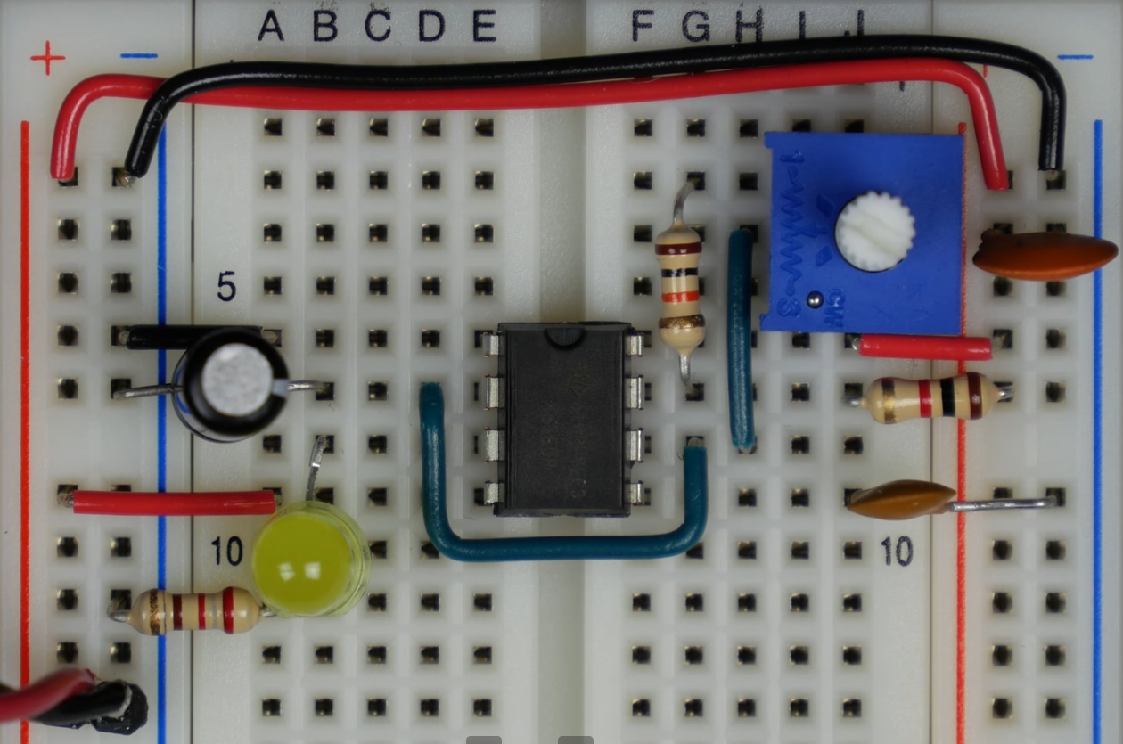
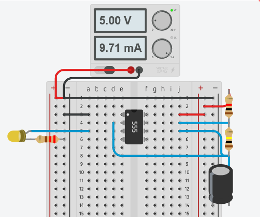
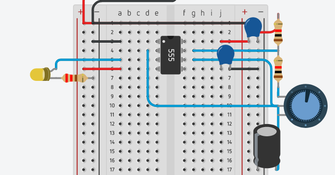
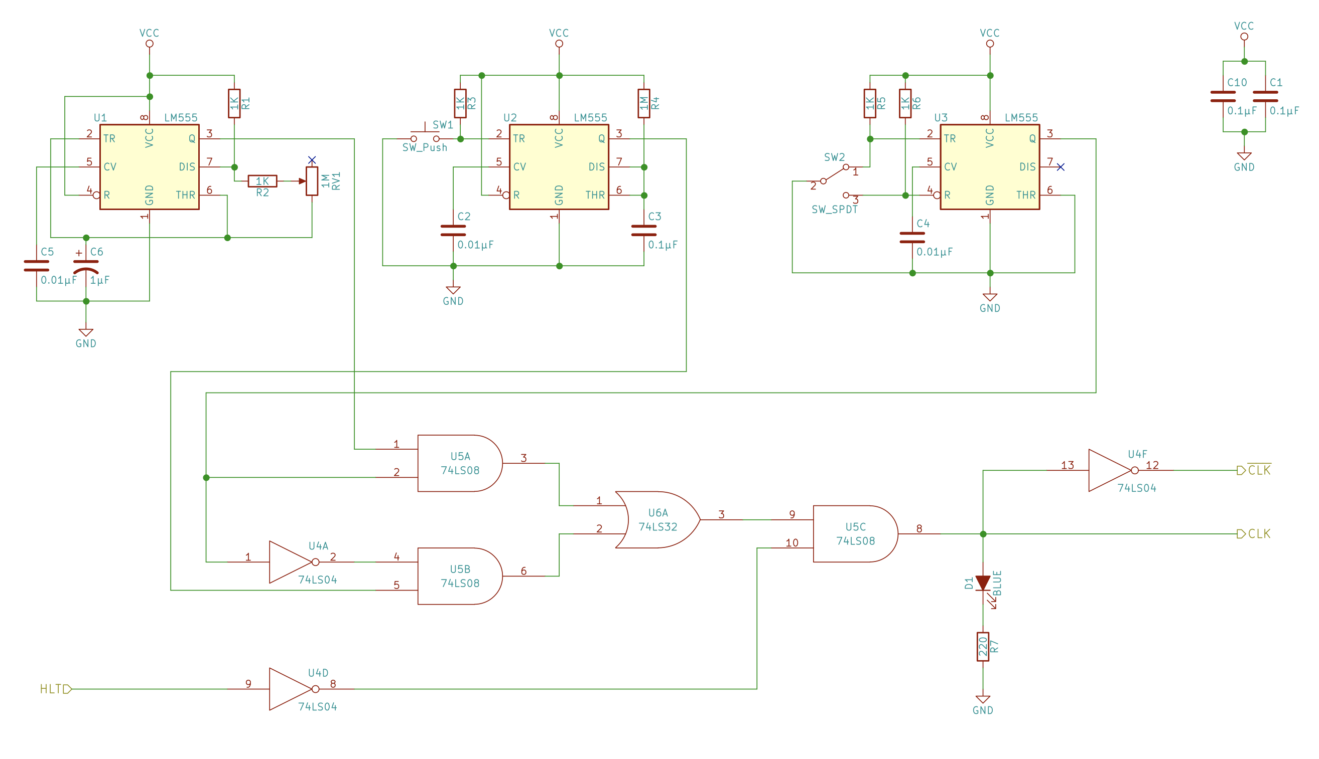
Astable 555 timer
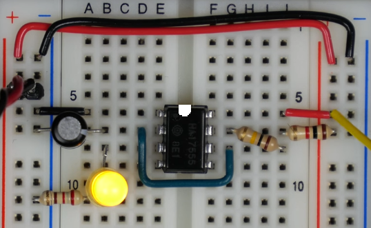
- We control the timing with 2 resistors and a capacitor
- The resistor connected from \(V_{cc}\) to pin 7 is of \(1k\Omega\)
- The resistor from pin 7 to pin 6 has \(100k\Omega\).
- The capacitor from pin 2 to ground is \(1\mu F\) (whose negative terminal is connected to ground)
- The breadboard rails are +5V and 0V (ground) although the voltage range of the 555 timer is typically 4.5 to 16 volts.
- The output of the 555 timer is around 3.3V and at least 2.75V
- The LED is connected to the output pin (3) and with a \(220\Omega\) as the current comming out of the output pin might burn it. The LED should alternate between on and off.
- It is called astable because it always alternates states
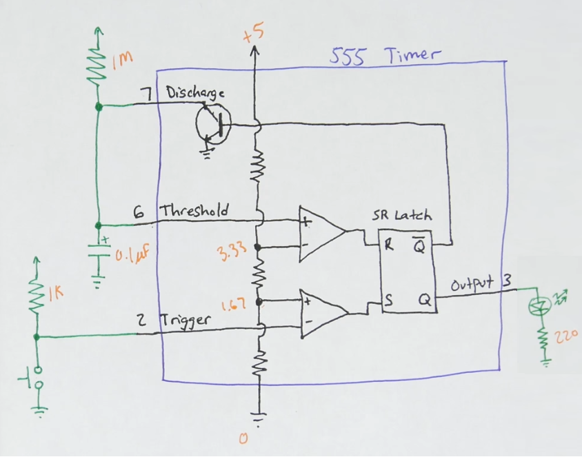
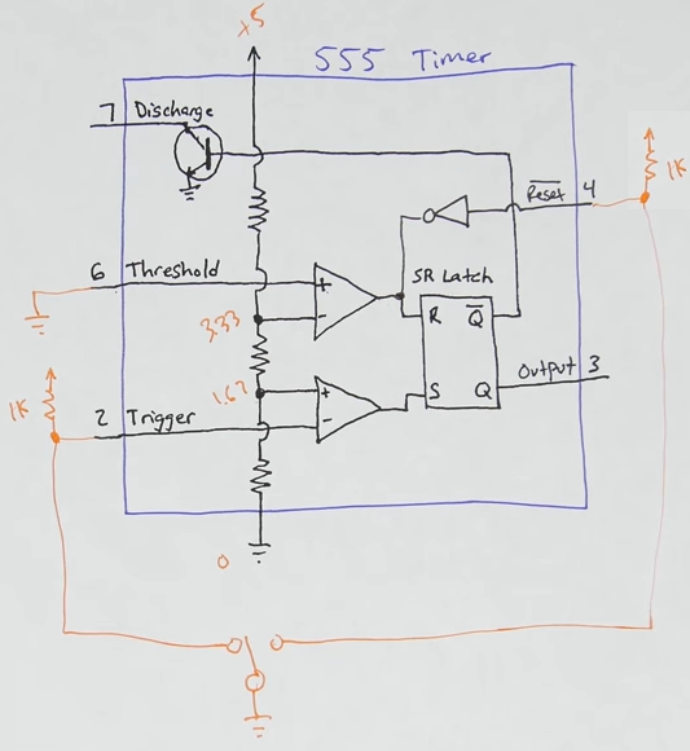
Schematic
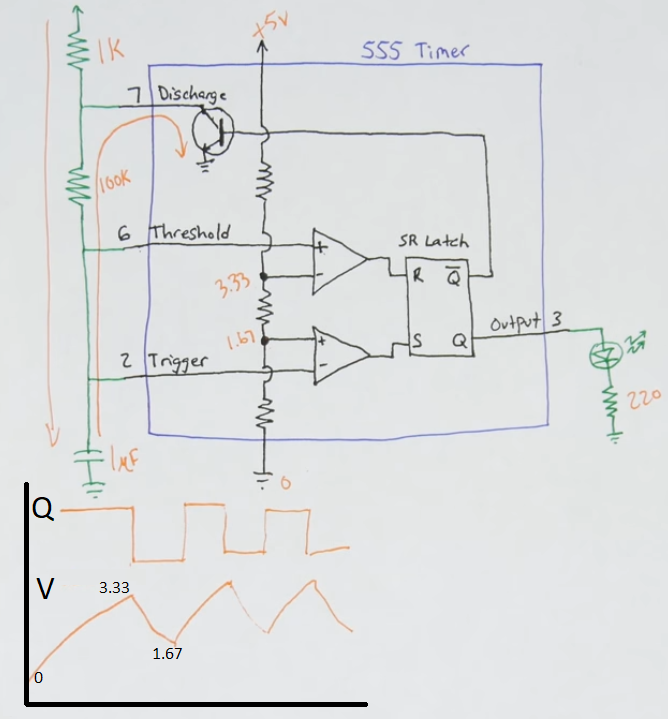
- The opamps (triangles with +-) are in a comparator setting
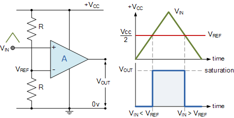
- The comparator output signal specifies whether the voltage input (\(v_{in}\)) is above (\(v_{out}=1\)) or below (\(v_{out}=0\)) the reference voltage (\(v_{ref}\)).
- The 3 resistors inside the 555 timer are probably \(5k\Omega\) each and they form a voltage divider circuit
- Therefore with a 5V source the voltage drop of the bottom resistor is \(5V\cdot\frac{5k\Omega}{15\Omega}\approx 1.67V\) and the voltage drop of the 2 bottom resistors combined is \(5V\cdot\frac{10k\Omega}{15\Omega}\approx 3.33V\) (recall that all voltage values are given in relation to ground).
- Therefore the reference voltage of the top comparator is 2.33V and the input voltage of the bottom comparator is 1.67V
- Therefore with a 5V source the voltage drop of the bottom resistor is \(5V\cdot\frac{5k\Omega}{15\Omega}\approx 1.67V\) and the voltage drop of the 2 bottom resistors combined is \(5V\cdot\frac{10k\Omega}{15\Omega}\approx 3.33V\) (recall that all voltage values are given in relation to ground).
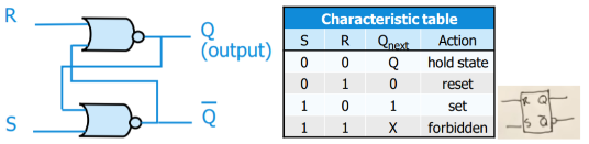
- You can also see that the output of the comparators feed the R and S terminals of an SR latch
Step response
- Assume the initial voltage of the capacitor is 0V and that the circuit has been powered off for a while
- The bottom comprator has \(v_{in} = 1.67V\) and \(v_{ref} = 0V\) as the capacitor had 0 energy stored. Since \(v_{in} \gt v_{ref} \implies v_{out} = High \implies S = 1\)
- The top comprator has \(v_{in} = 0V\) and \(v_{ref} = 3.33V\). Since \(v_{in} \lt v_{ref} \implies v_{out} = Low \implies R = 0\)
- From the truth table we see that S = 1 and R = 0 yield a high Q.
- \(\overline{Q}\) will be low and the transistor connected to pin 7 will not conduct.
- The capacitor starts increasing its voltage and at the beginning it’s low enough such that both comparators mantain the previous output but as soon as the capacitor reaches a voltage higher than 1.67 the bottom capacitor has \(v_{in} \lt v_{ref} \implies v_{out} = Low \implies S = 0\)
- While the capacitor has a voltage between 1.68 and 3.32 the top capacitor will keep \(v_{in} \lt v_{ref} \implies v_{out} = Low \implies R = 0\)
- SR = 00 means that Q which mantain whichever state it had, which in this is case was high and therefore \(\overline{Q}\) will be kept low and the transistor connected to pin 7 wont flow yet.
- As the capacitor surpases 3.34 the top comparator will have \(v_{in} \gt v_{ref} \implies v_{out} = High \implies R = 1\)
- SR = 01 means Q is low and \(\overline{Q}\) is high. The LED is now off.
- Since \(\overline{Q}\) is high the transistor will be connected to the branch emerging after the \(1k\Omega\) resistor, which since connects directly to ground it has zero resistance and all the current the previously flowed down pins 6, 2 and the capacitor won’t flow there as all of it will be discharged in pin 7
- Similarly the capacitor is also connected to the low resistance (although it has to go through a \(100k\Omega)\) resistor, recall that the inputs of an opamp have a very large resistance (not explicitly stated in the circuit), therefore the capacitor will also discharge via pin 7, and it’s voltage will start to drop.
- The top comparator will be the first one to switch from hight to low output, which would leave SR = 00, and mantain the current status quo.
- As the voltage of the capacitor drops below 1.66 volts the bottom comprator will switch from low to high output, which leaves SR = 10, which sets Q high (LED is back on) and \(\overline{Q}\) is low, which disconnects the discharger and everything is set back to the starting point (except that the capacitor might not have been fully discharged before it starts charging againg)
- While the capacitor has a voltage between 1.68 and 3.32 the top capacitor will keep \(v_{in} \lt v_{ref} \implies v_{out} = Low \implies R = 0\)
Speed
- The flashing frequency of the led is determined by Q which is determined by how quickly the capcitor charges and discharges
- This is determined by how much current flows into the capacitor
- The more resistance in the resistors, the less current flowing into the capacitor and the slower it’s going to charge (and also the slower it’s going to discharge as fewer current will be travelling back to the discharger)
- The larger the capacitance the longer it takes to charge/discharge. From here it follows that the bigger R * C the slower the clock
- The reason Ben has chosen 1k and 100k resistors is because charging will go through 101k resistance and discharging through 100k resistance making the high and low Q values of almost identical time.
- The charge time (Q output high) of the 555 timer given by its data sheet is: \(t_1=0.693(R_a + R_b)C\) with \(R_a\) being our 1k resistor and \(R_b\) the 100k one.
- Discharge time (Q output low): \(t_2 = 0.693 \cdot R_b \cdot C\)
- The total period is \(T = t_1 + t_2 = 0.693(R_a + 2R_b) C\) which in our case is 0.139 s
- The frequency (of oscillation) is \(\frac{1}{T}=\frac{1}{0.139}=7.19\) which means that the LED is flashing about 7 times per second
- We can replace the 100k resistor with a 1k resistor and a potentiometer in series (so when the potentiometer has 0 resistance there’s at least a 1k ressitor between pin 6 and 7) to manually adjust the speed of the clock
Noise
- Adding a \(.01\mu F\) capacitor from ground to pin 5 is recommended by the 555 timer datasheet as it clears the noise from low to high
- Our power supply (typically with curled wires) may act “not perfect” (i.e. as an inductor sometimes) and sometimes components (specially transistors) might get more volts than they actually desire at times.
- Adding a \(.1\mu F\) capacitor parallel to the power supply (i.e each leg on a + and - hole respectively in the breadboard) may help reduce dangerous voltage jumps.
- Ideally you’d want to have this capacitor right next to the power pins of the chip but there aint that much space in a breadboard.
- Low voltage on pin number 4 triggers a SR = 01 that overwrites whatever is going on with the comparators and resets (turns off) the SR latch. Therefore the datasheet recomends to hookup pin 4 directly to 5V power supply
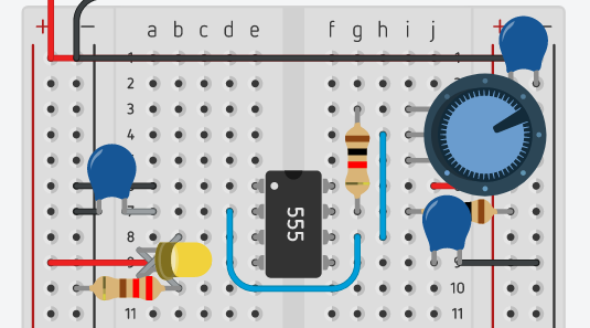
When we add all the noise and manual speed adjustments we end up with the following breadboard:
Tinkercad
-
Tinkercad of the original schematic
 Open tinkercad
 - Tinkercad of the upgraded circuit
- \(1M\Omega\) Potentiometer in series with Resistor B, which it decreases from \(100k\Omega\) to \(1k\Omega\) to manually adjust the speed.
- \(.1\mu F\) capacitor parallel to power supply to control voltage spike noise
- \(.01\mu F\) capacitor from ground to pin 5 to control low to high clock signal noise
- \(V_{cc}\) to pin 4 to avoid unvoluntary clock resets
 Open tinkercad
- Ben replica
- (Not inteded to implement in real life) Replaced the polarized capacitor with a small capacitor as it takes less space on the breadboard (it still has \(1\mu F\)).
- Shifted (aesthitically only) components to take less space.
- Placed everything on the breadboard
 Open tinkercad
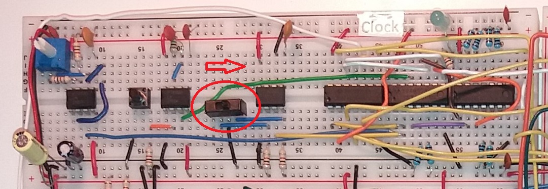
Monostable 555 timer
- We want to be able to manually advance 1 clock cycle
- Although a simple pushbutton seems to be enough to create cycles
- In reality the push button mechanics might unvoluntarily create additional clock cycles as the metal bounces additional times, not susceptible to the human eye
- In reality the push button mechanics might unvoluntarily create additional clock cycles as the metal bounces additional times, not susceptible to the human eye
- A debouncing circuit deals with this issue
- The duration of the high signal is determined by the capacitance times resitance of the two components on the right.
- It is called monostable because it only has 1 stable status (low)
Schematic
- Like the previous 555 timer circuit, there’s a resistor connected to pin 7 (discharge), but here it is also directly connected to pin 6 (threshold) as there is no resitor “b”.
- The capacitor (which determines the duration of the signal together with resistor a (the \(1M\Omega\) one), is also connected directly to pin 6 and 7
- The output lights a LED in series with a \(220\Omega\) resistor.
- Pin 2 is connected to a node that has a \(1k\Omega\) resistor directly connected to \(V_{cc}\) on the positive terminal and a push button directly connected to ground on the negative terminal
- I’ts like a voltage divider with \(R_1\) being 1k resistor and \(R_2\) the switch.
- \(v_0=v_s\frac{R_2}{R_1+R_2}\)
- When \(R_2\) is an open circuit it has infinity resistance, which gives \(v_0=v_s\frac{\frac{R_2}{R_2}}{\frac{R_1}{R_2}+\frac{R_2}{R_2}}=v_s\frac{1}{\frac{1}{\infty}+1}=v_s\)
- When \(R_2\) is a short circuit then \(v_0=v_s\frac{0}{R_1+0}=0\)
- When the push button is open, the voltage of pin 2 is \(v_{cc}\)
- The bottom comparator sends output 0 = S (which either resets or leaves current state)
- When the push button is closed, the voltage of pin 2 is 0
- The bottom comparator sends output 1 = S (which then sets the SR latch and triggers a high output
- I’ts like a voltage divider with \(R_1\) being 1k resistor and \(R_2\) the switch.
Step response
- Initally the push button is open so the bottom comparator sets S = 0, the LED is off and so is \(\overline{Q}\) high, which enables the discharge transistor. The capacitor which has 0V, is not able to charge, therefore the top comparator will mantain R = 0. The current state is kept (led off) until we intervene
- Only after pushing (and release) the button we can triger SR = 10 as we made the voltage of pin 2 to be 0 and hence the bottom comparator is able to set S = 1, which makes Q high and \(\overline{Q}\) low.
- This disables the discharge transistor and allows the capacitor to increase its voltage, the capacitor increases its voltage and when it’s above 3.34V it will reset the clock (given that the pusshbutton is not held on, otherwise we encounter SR = 11 which in an SR latch is an illegal configuration (it gives unpredictable output))
- As long as we dont deliberately hold the push button for too long this implementation should deal with the noise from the push button bounces
- After the capacitor triggers the reset, \(\overline{Q}\) becomes high and enables the discharge again, since there is no resistor between discharge and the capacitor it will bleed out it’s voltage very quickly, which immideately sets R back to 0.
- Therefore it’s very unlikely to achieve SR = 11 by doing very fast clicks (or rebounds), it should only possible by deliberately holding the button

- Therefore it’s very unlikely to achieve SR = 11 by doing very fast clicks (or rebounds), it should only possible by deliberately holding the button
Noise
Datasheet recomends:
- \(.01\mu F\) capacitor from ground to pin 5
- 5V to pin 4
Tinkercad
-
Tinkercad of the original schematic
 Open tinkercad
 -
Ben replica (with noise upgrade)
 Open tinkercad
Bistable 555 timer
- We could use a switch to manually alternate between the high and low clock output states
- However if we just use a mechanical switch we face the same rebound issue
- Since the 555 timer has a built-in SR latch, we can we can use it to set/reset the clock style as it also acts as a debouncer (because it latches the last state).
- We use a switch that is “break before make”

- The bouncing is always between the next step and the break, so any bouncing is not harmful as the desired result has been already latched as we’ll show below
- We use a switch that is “break before make”
- It is called bistable because both high and low output states are latched
Schematic
- We connect the threshold pin to the ground and just use the trigger pin (2) to set S = 1 (via the bottom comparator) and the reset pin (4) to directly (skipping the top comparator) set R = 1
- Since threshold is always below 3.33, R will always be 0 except when deliberately using the reset pin.
- Basically we need to send a low signal either to pin 2 (because it is inverted) xor pin 4 (because we want the trigger input of the comparator to be lower than 1.67) to set and reset respectively.
- Since we have a break-before-make switch, we will either:
- Connect pin 2 to ground (and make it 0V instead of the previous \(V_{cc}\)), which sets S = 1
- Break (neither pin 2 nor 4 are connected to ground): hold state
- Pin 2 has \(V_{cc}\) and therefore S = 0
- Reset pin is an open circuit and therefore doesn’t overwrite the top comparator, who always outputs low, so R = 0
- Connect pin 4 to ground and set R = 1
- The \(1k\Omega\) resistor on pin 4 is to connect 5V to pin 4 as recommended by the 555 datasheet and we use a resistor instead of just a piece of wire as pin 4 is also connected to ground and we do not want a short circuit.
- Not included in the schematic is the \(.01\mu F\) capacitor from ground to pin 5
Tinkercad
-
Tinkercad of the original schematic
 Open tinkercad
 -
Ben replica
 Open tinkercad
- Sometimes the switch icon might have an off starting image but tinkercad starts by default in the on position, so if things don’t seem to match at first glance just click once and the switch image will match the switch value
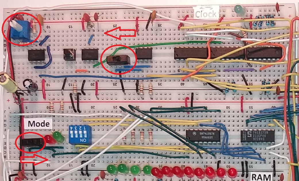
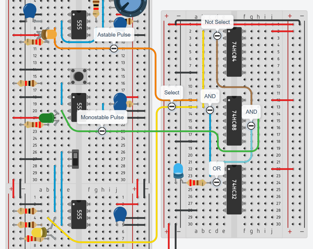
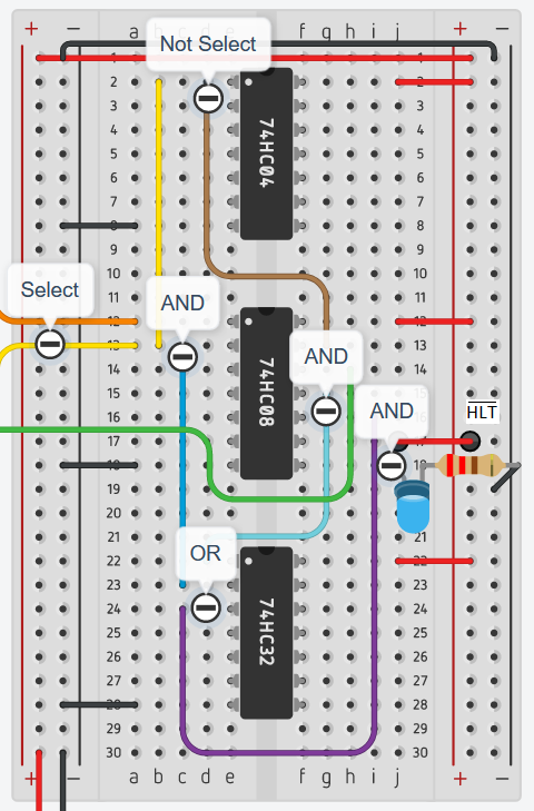
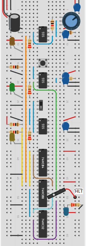
Clock logic
- We want to have one single clock output terminal that can be configured to either be a copy of the astable (automatic) or monostoable (manual) clock signal.
Logic circuit
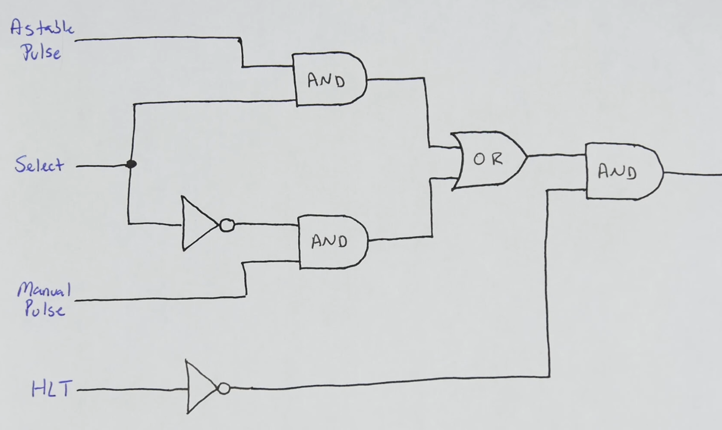
- HLT stands for halt signal (which can be send by programs) to stop the clock
- Latches low clock signal when we send a high voltage in HLT
- Low voltage does not interfere with the regular clock logic (described below)
- The logic circuit uses the bistable (called “select” in the schematic) clock just as a debounced switch, so the circuit is just to alternate between using the monostable clock (manual) and the astable clock (automatic)
- Because of the inverter of the select signal, exclusively and always one of the AND gates feeding from the clock signals will output a high voltage
- Take away:
- High bistable switch = astable
- High bistable and monosstable push = astable signal (the push is ignored)
- Low bistable switch = monostable
- high HLT (halt) = low clock signal until unhalted (then back to the previous clock setting)
- High bistable switch = astable
Components
- 1 74LS04 hex inverter
- Contains 6 inverters (we need 2)
- 1 74LS08 quad AND gate
- Contains 4 and gates (we need 3)
- 1 74LS32 quad OR gate
- Contains 4 or gates (we need 1)
- It would have been more efficient to rewrite the circuit with NAND gates and just use 2 74LS00 NAND chips (to use 7 out of 8 nand gates) but we’re not trying to optimize for power nor space but for understanding and maintanence.
- Tinkercad uses 74HC chips, which are slightly different than the 74LS chips shipped by Ben:
- 74LS need 5V \(V_{cc}\) and output a high voltage of 3.4V and a low voltage of 0.2V
- 74HC accepts from 2V to 6V and outputs with an output between 0 and \(V_{cc}\)
- Both have the same pin outs and most 74LS logic chips have internal resistors that let you connect LEDS directly to the outputs without a resistor. However, 74HC generally not.
- Therefore the tinkercad implementations have a \(220\Omega\) resistor in series with output LEDs.
Tinkercad
-
Tinkercad of the logic circuit without the HLT inverter and last AND gate.
 Open tinkercad
 - Tinkercad with the HLT inverter and last AND gate.
- Just plugs the output of the OR gate into an AND gate that for now takes the other input from a jumper cable either to ground (halt) or \(V_{cc}\) (not halt).
 Open tinkercad
- Just plugs the output of the OR gate into an AND gate that for now takes the other input from a jumper cable either to ground (halt) or \(V_{cc}\) (not halt).
- Simplified aesthetic circuit(with 74HC and \(220\Omega\) resistors) has the same logic connections:
- (Astable out, AND gate In 1A) - orange
- (Bistable out, AND gate IN 1B) - yellow
- (Bistable out (or AND gate in 1B), Inverter gate In 1) - yellow
- (Inverter gate Out 1, AND gate In 4B) - brown
- (Monostable out, AND gate In 4A) - green
- (AND gate out 1, OR gate In 1B) - dark blue
- (AND gate out 4, OR gate In 1A) - light blue
- (OR gate out 1, AND gate in 3A) - purple
Schematic
- Note: I ended up inverting the halt input as suggested by the schematic here
Testing the clock
- The clock can be fully tested in tinkercad by starting a simulation
- In real life the only adjustment I might need is to fix double bouncing of the push button, which happens occasionally.
- However it doesnt seem to be a capacitor resistor/555 timer issue as I can clearly notice the double clock pulse with the naked eye. It seems to be a mechanical issue, maybe I should replace the \(1k\Omega\) capacitor for a 10k one if the issue bothers me too much.
Registers
- Components included in the kit (including the components for ALU)
- 4 Breadboards
- 1 Jumper wire kit
- 6 25 foot hookup wire spools
- white
- blue
- green
- red
- yellow
- black
- 2 74LS86 quad XOR gate
- 6 74LS173 4-bit D register
- 4 74LS245 8-bit bus transceiver
- 2 74LS83 4-bit binary adder
- 40 \(220\Omega\) resistors
- 30 Red LEDs
- 10 Yellow LEDs
- 5 Blue LEDs
- 10 \(0.1\mu F\) capacitors
- Most CPUs (central processing unit) have a number of registers which store small amounts of data that the CPU is processing. In our breadboard CPU, we’ll build three 8-bit registers: A, B, and IR (instruction register)
- A and B are general-purpose registers
- IR will be used for storing the current instruction that’s being executed.
- The arithmetic logic unit (ALU) part of a CPU is usually capable of performing various arithmetic, bitwise, and comparision operations on binary numbers.
- Our ALU is just able to add amd substract
- It’s connected to the A and B registers
- Outputs either A+B or A-B
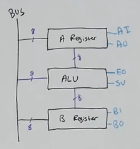
Bus architecture and how registers transfers work
- Our registers store 8 bits of data and interfaces (as in “provides interaction features”) to the Bus
- Most computers are organized around a Bus (or multiple)
- The Bus is basically a network of cables that connect multiple components within a computer.
- It’s a rather simple network, as the Bus serves primarly as a common connection point for multiple components within the computer
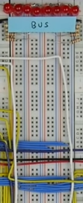
- For the 8 bit Bus we use 8 wires, and 4 snapped (+ -) power rails from 2 breadboards
- The way we use the bus is by one module writting data onto the Bus and another module reading data from the Bus
- Only 1 module can write data on the Bus at a time, otherwise the data carried on the bus is corrupted
- One of the main things a register does next to storing data is loading data onto the bus so other components can read it from the bus
- Registers have pins that when triggered with high/low voltage they can either read data from the bus or write it onto the bus.
- When “Enable” is high, the current data stored in the register is written (and overwrites) onto the bus. Then it’s visible to all the other modules (but they dont necessarily need to do anything with it)
- When “Load” is high, the register overwrites it’s current value with whatever value appears on the bus.
- Registers have pins that when triggered with high/low voltage they can either read data from the bus or write it onto the bus.
- The timing of each Load/Enable operation with the bus is synchronised by the clock signals as Load/Enable is gated with AND clock.
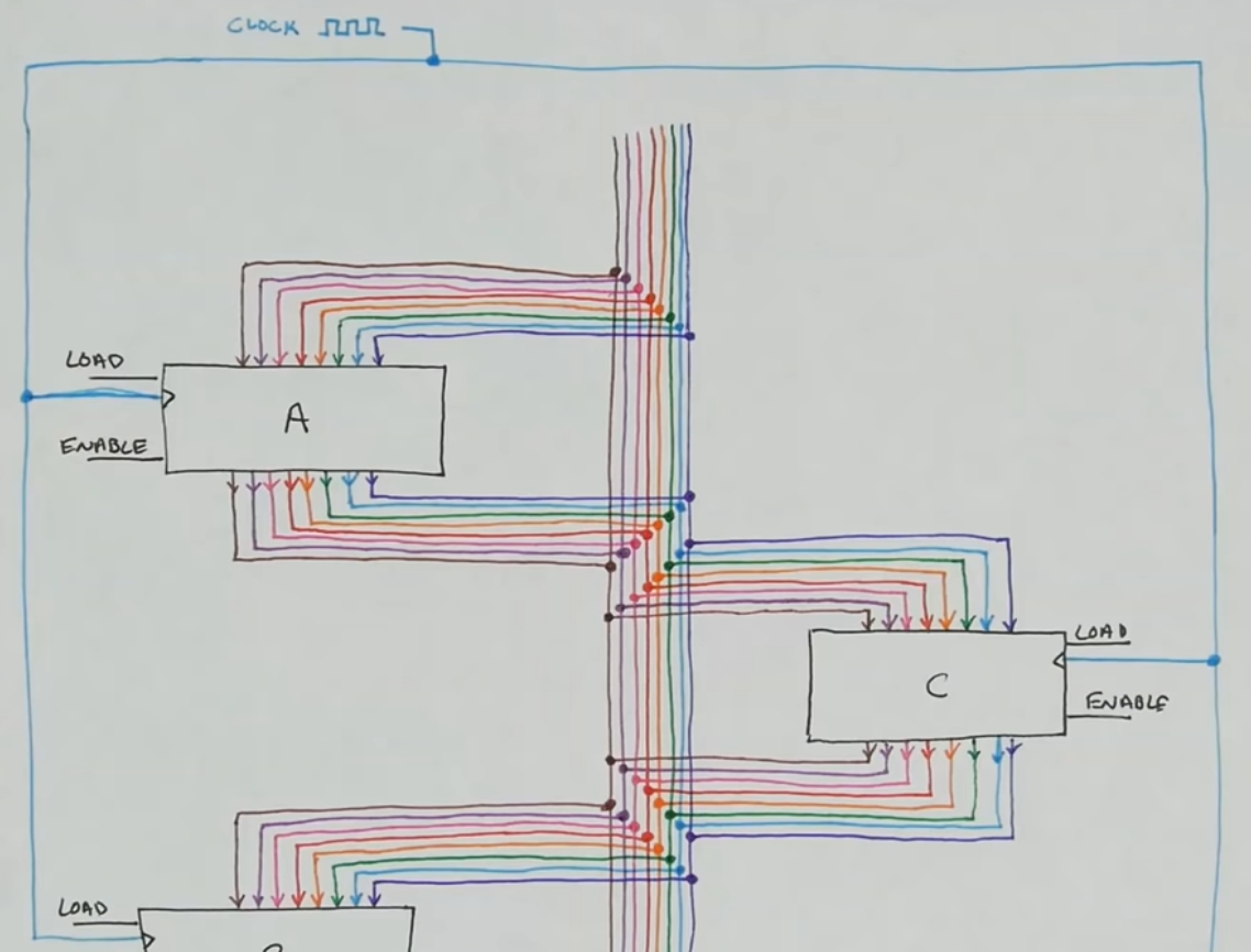
- Everything connected to the bus can potentially talk between all of them.
Connecting multiple outputs together
- The “Enable” output gates have some sort of transistor network that manages to either have an output that emits current from the pullup network (\(v_{cc}\) or an output that sinks current to the pull-down network (ground).
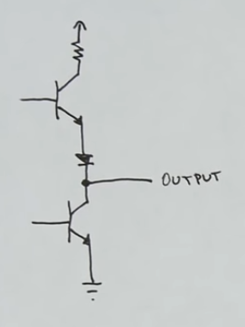
- The transistors above are NMOS (incomming high voltage closes the circuit)
- If top is high and bottom is low the output sources current
- If top is low and bottom is high the output sinsk current
- The load pins detect the current of the input pins connected to the Bus (which are connected to the register/component that is enabling its output pins) to determine whether the pin is a 0 (sinks) or a 1 (emits)
- This works well when only 1 component is emmiting/sinking current from the bus
- If component A emits all 1’s but component B is sinking all 0’s then component C will read a corrupted version of A’s data.
- Instead, the pull-up/pull-down transistor network for the outputs rather than having always closed circuit (either to ground or to \(v_{cc}\)), we can have a tri-state logic where we can just disconnect the output and leave an open circuit such that the outputs do not interfere with the Bus (unless enable is turned on, which shall be enabled by at most 1 component)
Tri-state logic
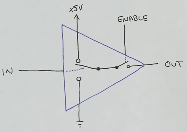
- If IN = 1, then switch is connected to \(V_{cc}\)
- If IN = 0, then switch is connected to ground
- If and only if enable is on, the output (a copy of IN) is connected to the bus
- So we end up with:
- Out = 0
- Out = 1
- Out = disconnected (does not overwrite the Bus)
- It is technically “high impedence” (with high resistance) as mechanically opening the circuit takes much more time and energy
- The input and output pins of the 74LS245 bus transceiver are connected to the enable pin a similar fashion
- We generally hide the pullup and pulldown network in the tri-state gate symbol
Designing and building a register
SR latch (store 1 bit)
- We can use an S-R latch with an enable button that specifies when SR can be fed into the SR latch
- When EN is 0, both AND gated output SR = 0, so the SR latch holds the previous state
- When EN is 1, the SR latch will get whichever values for S and R exist.
- We can create one single variable called D that feeds S and another branch of the same variable can be inverted and feed R. Therefore if D is 0 we get SR = 01, and if D is 1 we get SR = 10
D latch (just use 1 input)
- This is called a D-latch because it latches a single bit of data
D flip flop (latch at clock pulse)
- A D-flip flop would only latch a D value specifically when Enable is ON and when the clock switches from low voltage to high voltage (this prevents any other D changes during the same high clock signal cycle)
- This is technically enabling at each clock pulse
- We need an (edge detector) resistor capacitor (RC) circuit to produce a signal with very short high cycles (pulses)
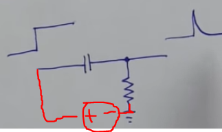
- The circuit above is such a circuit, which basically has a voltage as high as the source and behaves as the step response of a conductor-resistor circuit.
- Although at \(t_0\) (step from 0 to high voltage) the capacitor has 0V and behaves like a wire (\(I_s\) current), the voltage we are interested about is of the node connecting to the positive terminal of the resistor, which at \(t_0\) looks like \(R_2\) from a voltage divider where the inductor looks like \(R_1\) with \(0\Omega\) resistance, and thus \(V_0=V_s\) (high)
- The smaller the capacitance of the capacitor, the less it takes for the capacitor to charge, (and decrease it’s current), and thus the sooner the voltage drop of the capacitor reaches \(V_{s}\) and since it’s in series with the source the sooner it decreases the available voltage for all branches connected to \(V_{s}\) (KVL)
- According to to the RC constant:
- T = RC
- At 1T the voltage drop of fully charged capacitor in a natural response circuit is -37% (it’s providing voltage) of the initial voltage of the capacitor. The voltage drop of an empty capacitor in a step response circuit is therefore 63% of the source voltage (the resistor gets 37%)
- These are already considered significant enough to change a signal from logic high to logic low and viceversa
- After 5t the voltage drop is -1% of the initial source value in a natural response circuit (almost has no voltage to provide). In a step response circuit 5t makes the capacitor drop 99% of the source voltage (the resistor gets 1%)
- In a step response circuit the available voltage to the input pin will be the same as the one for the pull-down resistor, which will be \(V_{clock}\) minus the voltage drop of the capacitor. Overtime (5t) we see that the circuit is monostable until the clock signal is low again, but then the capacitor should discharge via the resistor (but when this happens it should not trigger a logic high because the voltage is not large enough for the chip to be considered high)
- AND gate output voltage (clock signal voltage) is typically 3.4V
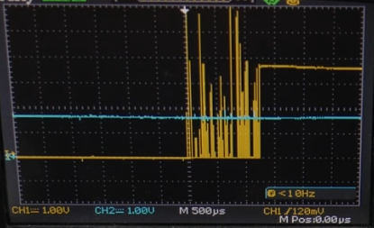
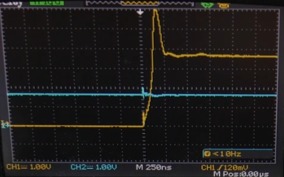
- At 1T capacitor drops 63% of the voltage, which makes it \(3.4V \cdot .63 = 2.04V\). The mux high level input voltage is 2V, so 1T is a good approximation for the time it takes to switch from high to low, but it’s slightly more than 1T as we could see.
- At 5T capacitor has 99% of the 3.4V, which when discharged should give another high signal. This explains the double clock pulse that other components experienced when this RC circuit shared the same clock signal, but then we used a diode for the branch of this RC circuit. It may be the case that in practice the RAM is doing double clock pulses, but it does not affect the functionality of the computer.
- \(0.1\mu F\cdot 1k\Omega\ = 0.1\cdot 10^6 F \cdot 10^3 \Omega = 0.1 ms\)
- According to to the RC constant:
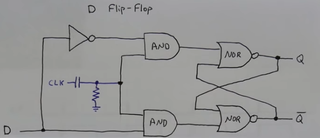
74LS74 (Two D flip-flops) and a load signal
- We can put several D flip flops together with some additional logic that write the contents of the bus when “Load” is high
- We can see that via the inverterter and the 2 AND gates linked to the load signal, the D bit fed to the D-latch is either the one of the bus when load is high, or the one latched when the load is low
- We can use 4 74LS74 chip which have 2 d-flip flops each built into it to make an 8-bit register
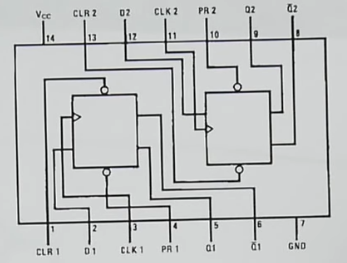
- GND: ground
- \(V_{cc}\): positive supply terminal
- CLRn: overwrites Bit n to 0
- PRn: overwrites Bit n to 1
- Flip flop pins: Dn (bus’ n bit), CLKn, Qn, \(\overline{Qn}\)
- Tinkercad implementation of 1 bit register
- It only allows register changes at clock rise (blue led on) and when load is high
-
We still need to add the tri-state buffer to the output of the register to ensure we dont corrupt the bus when we’re not using it
- Alternatively we can use the 74LS245.
74LS245 (Octal bus transceiver used as tri-state logic gate)
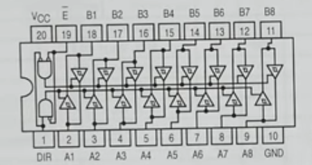
- Useful for sending bus data in both directions
- Pin 1 is for direction control (whether the register sends data or whether the bus sends data)
- Because we already use the load variable to determine when to read from the bus we just need to use the feature to send (An pin to Bn pin), so we set pin 1 high.
- Pin 19 is “enable”, which is the tri-state logic “switch” that connects/disconnects us from the bus
74LS173A (4 bit registers)
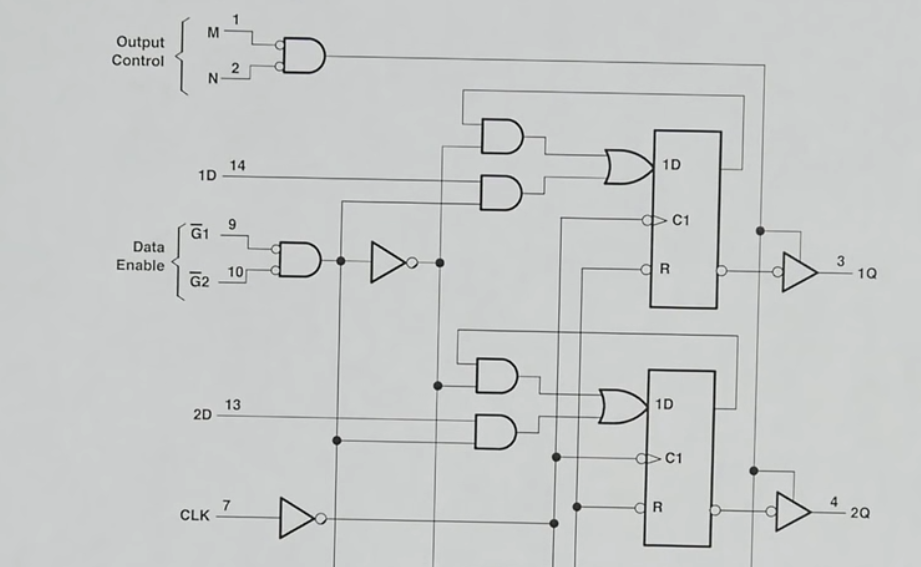
- 4 built-in D flip flops
- Uses similar logic of having a sequence of flip-flops connected to the bus and written when a load signal (called enable) is high
- Built-in tri-state output with output control pin
- Used in this project as building multiple 8 bit registers with just basic logic gates is a cumbersome repetitive process not necessarily in line with the goal of the project.
Building an 8-bit register
- We will be using 2 74LS173A chips for each 8 bit register
- It has a built-in tri-state logic gate with the default output set to be disconnected unless the output control is enabled
- Since we want to be able to see at all times what’s the value of the register, we will turn the output cotroll to be always enabled, put a LED in series, and then manually add another tri-state logic gate with the 74LS245.
- The 74LS173A requires both M and N to have 0V (grounded) to output the contents of the 4-bit
- The 74LS173A also has 2 inverted load inputs per pin, so does the enable pin of the 74LS245.
- Low \(\overline{\text{ENABLE}}\): register output is sent to the bus
- High \(\overline{\text{ENABLE}}\): register output is not sent to the bus
- Low \(\overline{\text{LOAD}}\): bus content is sent to the register
- High \(\overline{\text{LOAD}}\): bus content is not sent to the register
- If you do things right, you will never have a high load and a high enable at the same time (that is, sending to the bus and reading from the bus at the same time is an unlikely scenario)
- CLR: resets bits to 0, should be set to ground rather than open.
- DIR: we always set it high such as the the direction of the tri-state logic gate is always from
Tinkercad
- Tinkercad implementation.
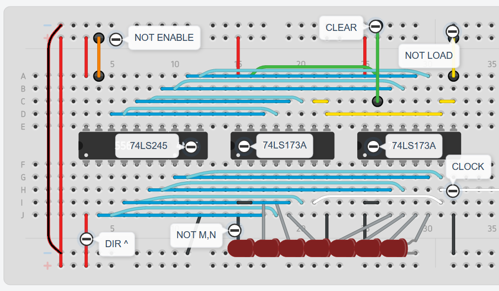
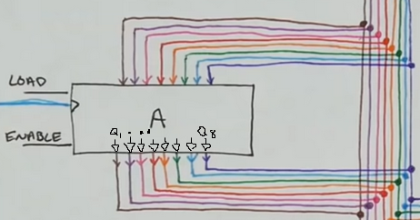
- Bus to register: The inputs of the registers (who have not load pin low (load = 1) in this context) are connected to the outputs of the tri-state logic gate (who has not enable pin high (enable = 0)) that connects to the bus (light blue cables)
- Register to Bus: The outputs of the registers are always connected (M, N, pins to ground so we can see the register contents with the LEDs) to the tri-state logic gate (who has not enable pin low (enable = 1) in this context) such that it can be sent to the bus (green cables)
- Bus to register: The inputs of the registers (who have not load pin low (load = 1) in this context) are connected to the outputs of the tri-state logic gate (who has not enable pin high (enable = 0)) that connects to the bus (light blue cables)
Schematic for Register A (same as B)
- AI = Load
- AO = Enable
- \(A_n\) = input for the ALU A’s n input
Schematic for Instruction Register
Testing the register with a temporary bus
- If there’s no connection to a bus and you set load high, the 74LS173A chip will default the inputs as high voltage as there’s typically a pull-up resistor, therefore all the bits of the register will set to 1 if there’s an open circuit with the bus
- This happened because load was high and enable was low (and since there’s only this register there’s literally no enabled bits in the bus, thus the bus is an open circuit (the input is floating and not grounded as although the Bus LEDs are connected to ground they are a diode, meaning that they are designed such that current only goes in one direction. Since the LEDs are aligned in a way to expect the current to come from the Bus, they are disallowing the situation where there are no current comming from the Bus and an input pin pull-up resistor wants to sink via the Bus leds connected to ground (that is not allowed as the LED blocks the current going that way, it essentially behaves then as an open circuit)))
- Later we will add a set of 8 \(10k\Omega\) resistors connected to the Bus and to ground to default the value of the Bus to 00000000 when there’s no party enabling the Bus.
- Since their resistane is significantly high, they should not sink in much current when the bus is enabled, thus not affecting the normal behavour of the Bus.
- Later we will add a set of 8 \(10k\Omega\) resistors connected to the Bus and to ground to default the value of the Bus to 00000000 when there’s no party enabling the Bus.
- This happened because load was high and enable was low (and since there’s only this register there’s literally no enabled bits in the bus, thus the bus is an open circuit (the input is floating and not grounded as although the Bus LEDs are connected to ground they are a diode, meaning that they are designed such that current only goes in one direction. Since the LEDs are aligned in a way to expect the current to come from the Bus, they are disallowing the situation where there are no current comming from the Bus and an input pin pull-up resistor wants to sink via the Bus leds connected to ground (that is not allowed as the LED blocks the current going that way, it essentially behaves then as an open circuit)))
- If we set the load low and the enable high we should be able to move the contents of the register to the bus
- Try to load a bus with some pins connected to ground such that the received load is a combination of 1s and 0s.
-
Then connect another register to the bus and transfer the contents (which should appear in the next clock cycle).
- My testing experience:
- The register outputs and Bus LEDs without resistors, although allowed by the LS chips, seemed to sink too much current due to their low resistance (and that next they are connected to ground), and I wasn’t able to send 8 ON bits from one register to the other until I removed the bits from the outputs and added a series \(220\Omega\) resistor to each LED in the Bus.
- Therefore my 8-bit computer will always have a resistor in series with each LED.
Instruction register
- The instruction register is identical besides that it is aestethically mirrored as we will place it on the left side of the computer
- Also it will only connect the 4 least significant bits (yellow) to the Bus, as the other 4 will connect to into the instruction decoder (next chapters)
- So you should connect A1-A4 (4 most significant bits) of the buffer to ground
- Make sure to connect to use the clock signal, which is the left leg of the RC capacitor of the RAM input module, and not the pull-down resistor.
Arithmetic Logic Unit (ALU)
Adding numbers
- Adding 2 bits has 4 logic variables:
- bit \(A_n\)
- bit \(B_n\)
- carry \(C_n\) also known as “carry in”
- carry \(C_{n+1}\), also known as “carry out” for \(A_{n+1} + B_{n+1}\) (and implicitly \(+ C_{n+1}\))
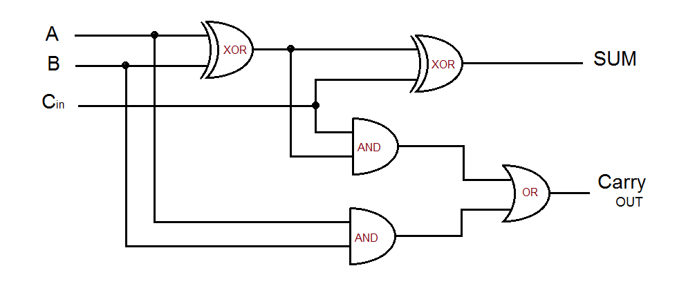
- You can replicate the same circuit k times to have a k-bit full adder (and use the last carry out bit to eventually display the most significant bit to not overlfow the result)
- The carry out of the adder \(n\) is the carry in of the adder \(n+1\)
4-bit adder (74LS283)
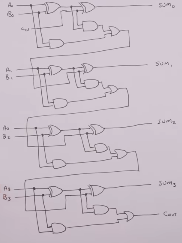
- The 74LS283 chip implements the same logic as above.
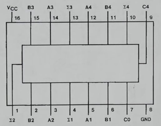
- C0 is the carry in
- C4 is the carry out, which we can use to cascade another 74LS283 4-bit adder
Negative numbers
- There are multiple ways to represent binary negative numbers
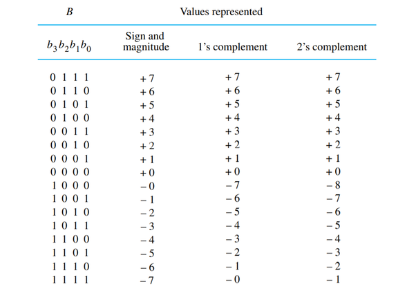
- Sign and magnitud: uses the most significant bit (MSB) as a sign bit, when such bit is 0 the number is positive, when the MSB is 1 the number is the same \(\cdot -1\)
- 1’s complement: Flips zeros and 1s (XOR all 1’s) to make the negative version
- 2’s complement: To make the negative version you XOR all 1’s and then XOR the least significant bit (LSB) with 1 (so 1 C’s negative + 1)
- 2’s complement is our choice to represent negative numbers since subtraction can use the same algorithm as addition.
- We just have to always ignore the last carry bit
- Overflow example: When 4 bit full adders sum 0111 (7) + 0001 (1) we end up with 1000 (-8)
- MSB is 1, so it’s negative
- flip(1000) = 0111
- XOR(1,0111) = 1000 = \(2^3\) = 8
- 1000 = -8
- MSB is 1, so it’s negative
- Therefore the range of 2’s complement is \([-2^{k-1}, 2^{k-1}-1]\)
ALU design
- Our ALU will only do addition and subtraction
- We will also connect the output of registers A and B directly to the inputs of the ALU
- It will output to the Bus either:
- A+B (\(EO\))
- E symbolizes \(\Sigma\), which is the sum
- A-B (\(SU\))
- SU symbolizes “subtraction”
- A+B (\(EO\))
- AI/BI stands for load bus to A/B (load A/B input from Bus)
-
AO/BO stands for enable A/B onto the Bus (enable A/B output to Bus)
- Just like with the registers, we don’t want to connect (and sink current) to the Bus at all times. We therefore also use tri-state logic gates to output to the bus (high, low or disconnect (aka not interact))
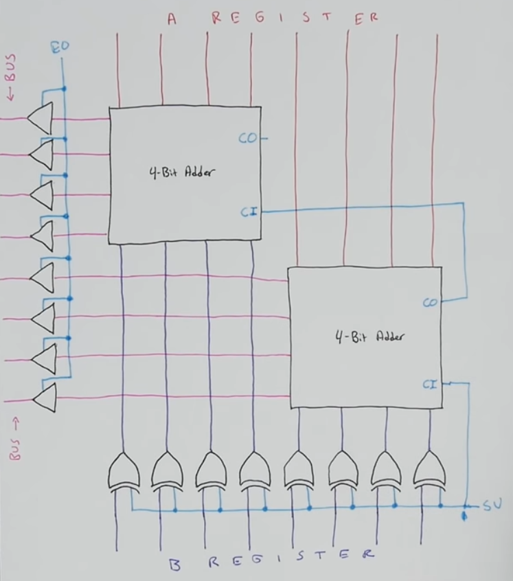
- The XORs gates for B outputs can be triggered with a unique signal that XORs B with all 1’s such that B is inverted, then to subract A-B we only need to do A + inverted B + 1 (2’s complement sum = subtraction)
- It’d be cumbersome to implement another full adder just to sum 1.
- Instead we can use the carry in bit of the least significant 4-bits adder and connect it together with the signal to XOR all 1’s such that the adder already takes care of finishing the negation in 2’s complement of B by summing 1 each time we decide to XOR all B’s outputs
- Therefore \(EO\) and \(SU\) are not exclusive instructions:
- \(EO\) high and \(SU\) low = output A+B
- \(EO\) high and \(SU\) high = output A-B
- \(EO\) low = disconnect from Bus
Building the ALU
- Components:
- 2 4-bit adders chips (74LS283)
- 2 XOR gates chips (74LS86)
- 1 tri-state buffer chip (74LS245)
- Steps:
- Connect power/ground pins of all ALU chips and DIR (\(V_{cc}\) to pin 1) of the tri-state buffer of the ALU
- Connect carry out of LSB adder (right C4) to carry in of MSB adder (left C0)
- Connect outputs of A register to ALU’s adders \(A_n\) inputs:
- The tri-state buffer pins of register A are BIG endian (the most significant bit (leftmost number) has the smallest address (A1)) while the adder is little endian (the least significant bit has the smallest address (A1))
- \(\text{Buffer}_A A_8\ (pin\ 9) = \text{LSB adder (right) } A_1\ (pin\ 5)\)
- \(\text{Buffer}_A A_7\ (pin\ 8) = \text{LSB adder (right) } A_2\ (pin\ 3)\)
- \(\text{Buffer}_A A_6\ (pin\ 7) = \text{LSB adder (right) } A_3\ (pin\ 14)\)
- \(\text{Buffer}_A A_5\ (pin\ 6) = \text{LSB adder (right) } A_4\ (pin\ 12)\)
- \(\text{Buffer}_A A_4\ (pin\ 5) = \text{MSB adder (left) } A_1\ (pin\ 5)\)
- \(\text{Buffer}_A A_3\ (pin\ 4) = \text{MSB adder (left) } A_2\ (pin\ 3)\)
- \(\text{Buffer}_A A_2\ (pin\ 3) = \text{MSB adder (left) } A_3\ (pin\ 14)\)
- \(\text{Buffer}_A A_1\ (pin\ 2) = \text{MSB adder (left) } A_4\ (pin\ 12)\)
- The tri-state buffer pins of register A are BIG endian (the most significant bit (leftmost number) has the smallest address (A1)) while the adder is little endian (the least significant bit has the smallest address (A1))
- Connect outputs of the adders to the tri-state gate inputs (of the ALU module):
- \(\text{Buffer}_{ALU} A_8\ (pin\ 9) = \text{LSB adder (right) } \Sigma 1\ (pin\ 4)\)
- \(\text{Buffer}_{ALU} A_7\ (pin\ 8) = \text{LSB adder (right) } \Sigma 2\ (pin\ 1)\)
- \(\text{Buffer}_{ALU} A_6\ (pin\ 7) = \text{LSB adder (right) } \Sigma 3\ (pin\ 13)\)
- \(\text{Buffer}_{ALU} A_5\ (pin\ 6) = \text{LSB adder (right) } \Sigma 4\ (pin\ 10)\)
- \(\text{Buffer}_{ALU} A_4\ (pin\ 5) = \text{MSB adder (left) } \Sigma 1\ (pin\ 4)\)
- \(\text{Buffer}_{ALU} A_3\ (pin\ 4) = \text{MSB adder (left) } \Sigma 2\ (pin\ 1)\)
- \(\text{Buffer}_{ALU} A_2\ (pin\ 3) = \text{MSB adder (left) } \Sigma 3\ (pin\ 13)\)
- \(\text{Buffer}_{ALU} A_1\ (pin\ 2) = \text{MSB adder (left) } \Sigma 4\ (pin\ 10)\)
- Connect outputs of B register to one of the inputs of XOR gates
- For simplicity, connect MSB bit with left XOR input B4:
- \(\text{Buffer}_B A_8\ (pin\ 9) = \text{right XOR input } 1B\)
- \(\text{Buffer}_B A_7\ (pin\ 8) = \text{right XOR input } 2B\)
- \(\text{Buffer}_B A_6\ (pin\ 7) = \text{right XOR input } 3B\)
- \(\text{Buffer}_B A_5\ (pin\ 6) = \text{right XOR input } 4B\)
- \(\text{Buffer}_B A_4\ (pin\ 5) = \text{left XOR input } 1B\)
- \(\text{Buffer}_B A_3\ (pin\ 4) = \text{left XOR input } 2B\)
- \(\text{Buffer}_B A_2\ (pin\ 3) = \text{left XOR input } 3B\)
- \(\text{Buffer}_B A_1\ (pin\ 2) = \text{left XOR input } 4B\)
- For simplicity, connect MSB bit with left XOR input B4:
- Connect all other inputs of the gates together (A inputs), as well as the “carry in” of the least significant adder (right C0)
- Connect a jumper wire connected to these conections to either \(V_{cc}\) or ground (this is our subtract signal)
- Connect outputs of XOR gates to adders \(B_n\):
- Remember to pair whichever XOR gate had Buffer B1 as an input with the MSB (left) adder B4 pin, etc.:
- \(\text{left XOR output 1} = \text{LSB adder (right) input } B_1\ (pin\ 6)\)
- \(\text{left XOR output 2} = \text{LSB adder (right) input } B_2\ (pin\ 2)\)
- \(\text{left XOR output 3} = \text{LSB adder (right) input } B_3\ (pin\ 15)\)
- \(\text{left XOR output 4} = \text{LSB adder (right) input } B_4\ (pin\ 11)\)
- \(\text{left XOR output 1} = \text{MSB adder (left) input } B_1\ (pin\ 6)\)
- \(\text{left XOR output 2} = \text{MSB adder (left) input } B_2\ (pin\ 2)\)
- \(\text{left XOR output 3} = \text{MSB adder (left) input } B_3\ (pin\ 15)\)
- \(\text{left XOR output 4} = \text{MSB adder (left) input } B_4\ (pin\ 11)\)
- Remember to pair whichever XOR gate had Buffer B1 as an input with the MSB (left) adder B4 pin, etc.:
- Connect enable jumper wire for the tri-state buffer
- Set the direction pin of the tri-state buffer high
- Connect the output of the tristate buffer of the ALU to the Bus
- Optional: hookup LEDs to the tristate buffer inputs of the ALU
Tinkercad
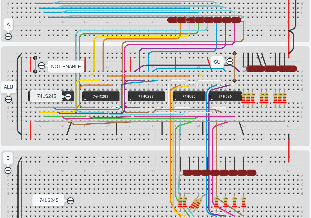 Open tinkercad.
Schematic
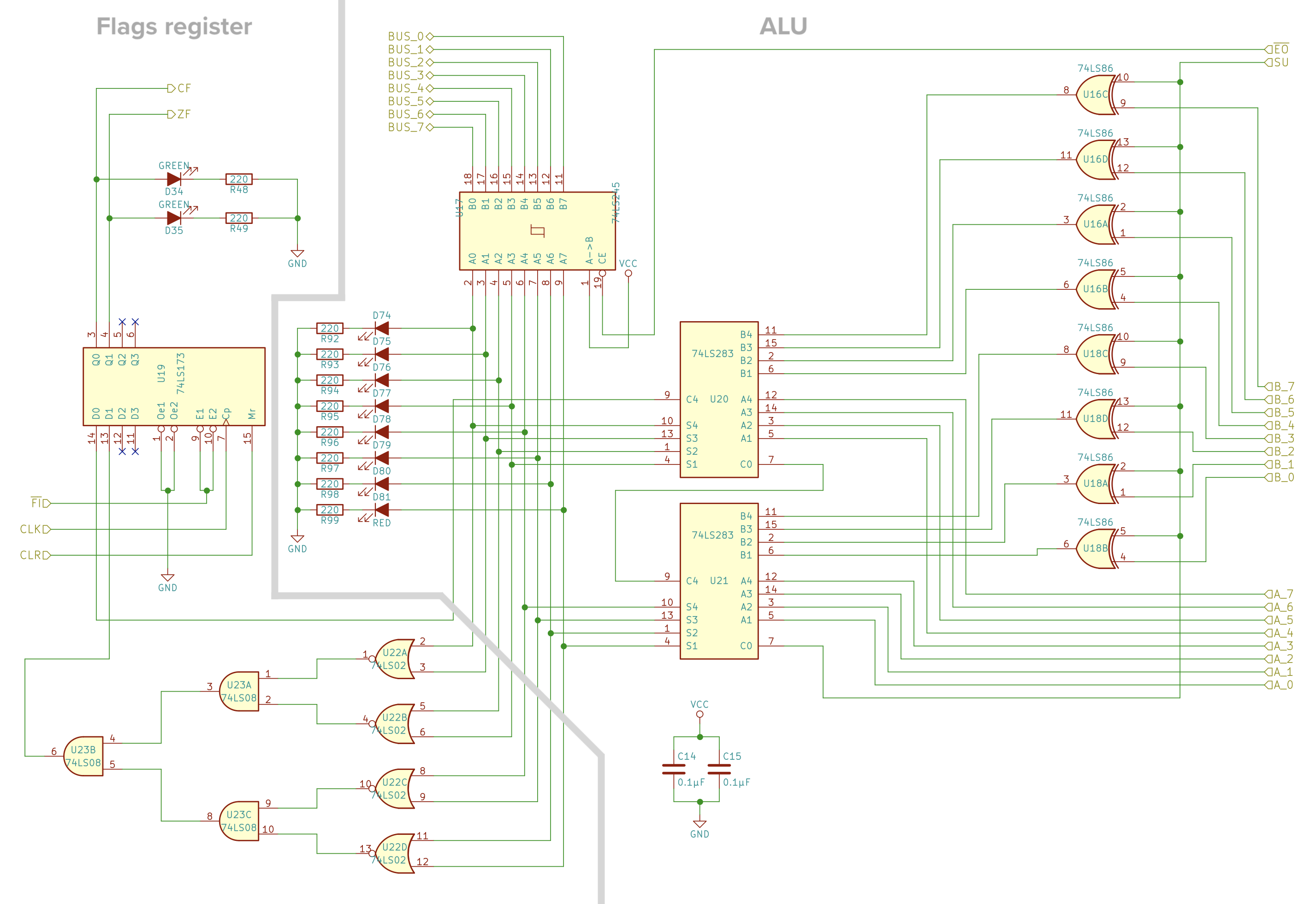
- The flags register portion of the schematic is described later on as part of the CPU control logic.
Testing the ALU
- Because the registers only load from the Bus at clock rise, if we ENABLE the ALU onto the Bus and LOAD the Bus onto a register, when we advance 1 clock cycle this will happens. If we are adding:
- at t0 (before advancing clock cycle) the Bus shows A+B (let’s say)
- then at t1:
- register A = ALU at t0
- ALU = A (which is ALU at t0) + B
- Bus = ALU (which is ALU at t0) + B
- This is basically Bus += b at each clock cycle
- If we only have LEDs hooked up to the bus, we can debug B++, A++, and B– in a similar fashion
- 1 clear the contents of both registers
- Load all 1s to register A (by having high load and nobody enabling the bus)
- Load all 1s except the least significant bit (by connecting that bit on the bus to ground) in register B
- The subtraction should be \(-1 –2 = 1\)
- Clear both registers and load the Bus (which has number 1) onto the register that you want to test (and its connection with the ALU)
- Peform the steps mentioned at the beginning of this section, and do all permutations of (A/B clear, the other with 1) x sum/subtract
- A– cannot be tested since only the sign of B can be changed with the SU signal
- Then you can also utilize the random D-latch starting values to generate test cases from those random boot register values with almost no setup costs.
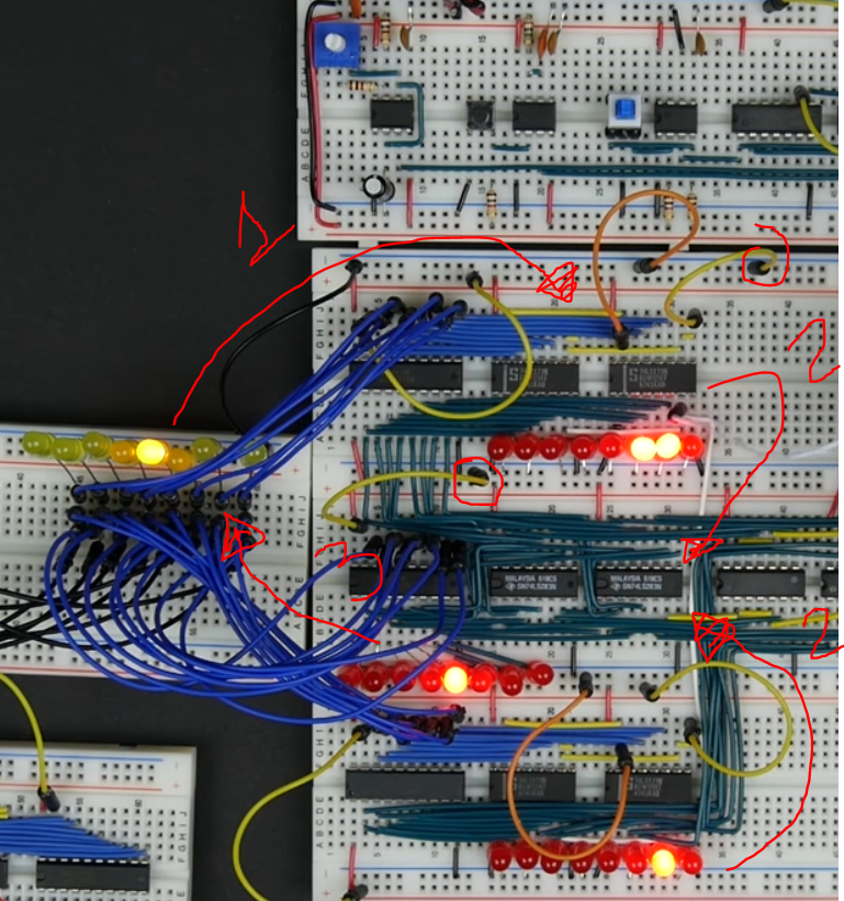
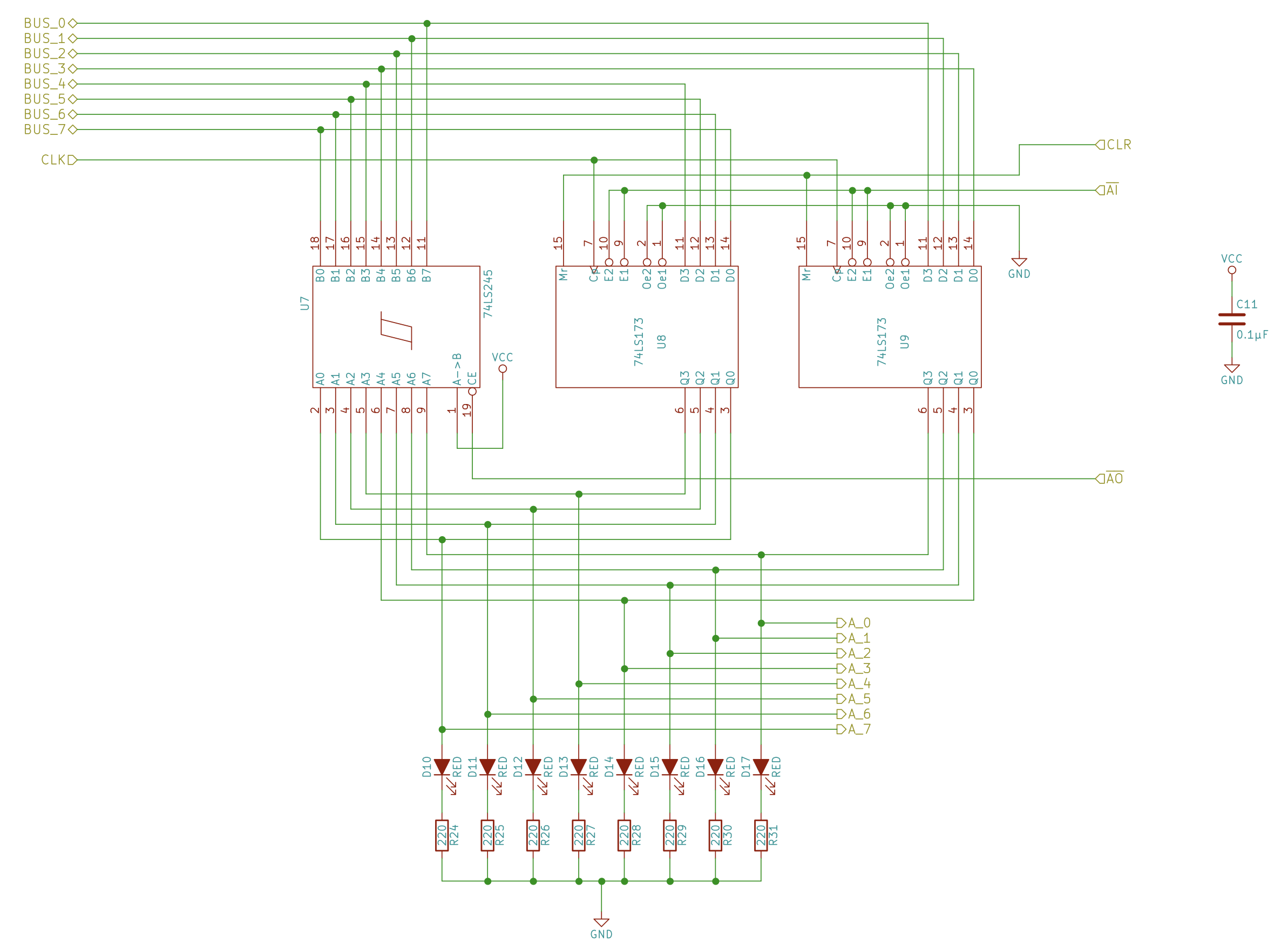
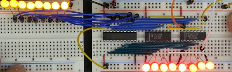
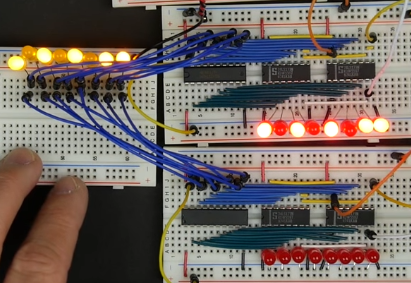
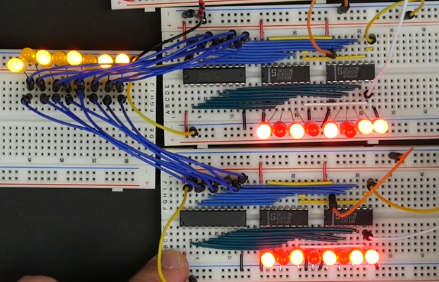
Random Access Memory (RAM)
- Components in the kit (including the program counter)
- 4 Breadboards
- 1 74LS00 quad NAND gate
- 2 74LS04 hex inverter
- 4 74LS157 quad 2-1 line mux (multiplexer)
- 1 74LS161 4-bit binary counter
- 1 74LS173 4-bit D register
- 2 74LS189 64-bit RAM
- 2 74LS245 8-bit bus transceiver
- 1 Pushbutton
- 1 Slide switch
- 1 4-position DIP switch
- 1 8-position DIP switch
- 20 \(220\Omega\) resistors
- 5 \(1k\Omega\) resistors
- 10 Red LEDs
- 10 Green LEDs
- 10 Yellow LEDs
- 5 \(0.01\mu F\) capacitors (103 code)
- 5 \(0.1\mu F\) capacitors (104 code)
- The random access memory (RAM) stores the program the computer is executing as well as any data that the program needs
Register recap
- We could store 1 bit of data with an SR latch, and on top of that, require an enable signal together with S and R signals
- SR 00 = keep value
- SR 01 = 0
- SR 10 = 1
- SR 11 = illegal state
- If not enable the two AND gates always yield SR 00 (keep value)
- A D-latch replaces the SR signals with a single data signal (D) which has 2 branches, the one that keeps the same signal goes to S gate, the inverted one goes to R. On top of that we can keep the enable signal with the same logic as before.
- This logic means that now we can still do SR 00 (low enable), SR 01 and SR 10 as before but not the illegal state SR 11 (which is a good thing to avoid that scenario as it serves no purposes and it’s impredictible).
- A D flip flop is an upgraed D-latch that only sets/resets a bit at a clock pulse (useful feature for better synchronization and less noise bugs)
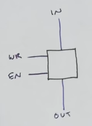
- We can group several flip flops together to make a register
- \(D_n\) = Input for bit n (usually connected to the Bus)
- \(\text{LOAD}\) = write onto the register signal (a separate “enable” signal independent from the clock signal, as the latter is already given explicitly by the arrow in the bottom left corner of the D flip flop box symbol)
- To finalyze the register we need an output signal that generally allows the register to output each of its bits to the Bus, to do so we use tri-state gates as we want all other outputs of the components not loading the bus to be disconnected from the Bus to avoid conflicts (we dont want a high signal from B overloading a low signal from A nor a low signal B sinking a high signal from A)
- In this context “IN” would be Q of a D flip flop of a register.
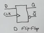
- A one bit register can be summarized with the symbol below
- An 8 bit register:
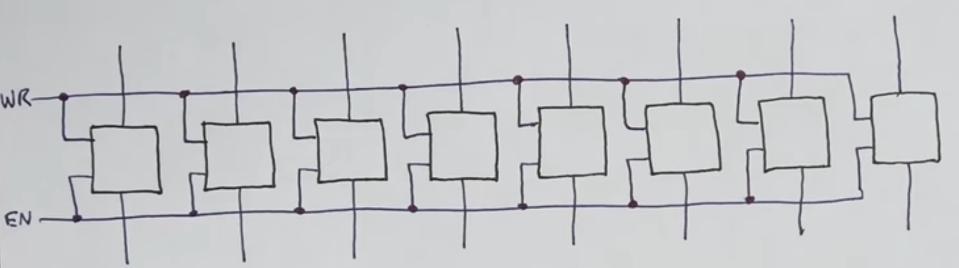
- A 16 byte ram would essentially be sixteen 8-bit registers packed into 1 chip
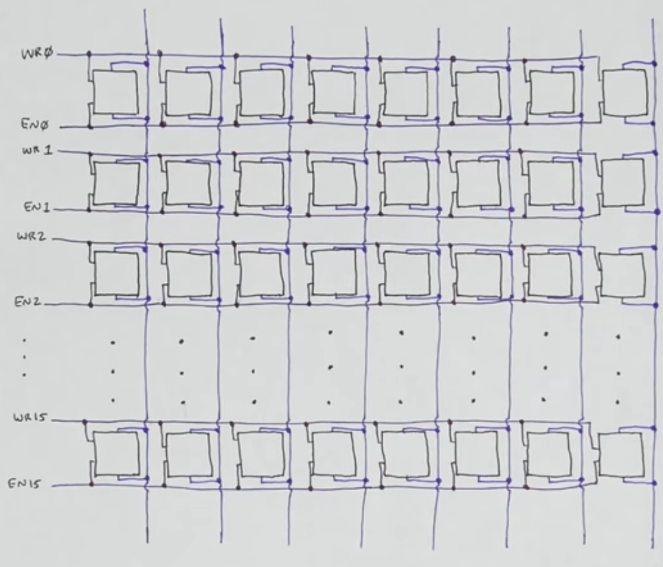
- With 16 write/enable (y-axis) and 8 (8 bits = 1 byte) data signals (x-axis)
- Each of those 16 registers (row), can be given a binary address and together with a decoder we can provide the high voltage signal to the specific register only.
- The decoder logic is great because in the context of chips, we can have a decoder inside and limit the amount of external pins needed for the users to specify an address.
DRAM vs SRAM
- Each of the bit cells that make up our RAM can be stored in a simpler circuit than a flip flop with just a transistor and a capacitor
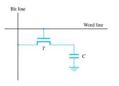
- When the capacitor is charged and the address is enabled (word line) the bit voltage is high
- When the address is enabled and the capacitor is not charged it behaves like a piece of wire with 0 voltage drop, and since it’s connected to ground the bit voltage is low
- Drawback: Overtime the capacitor discharges and can only store bits for a few seconds. It also has destructive read as each time we read the content of the bit we are sinking the voltage of the capacitor, so it must be recharged immedeately after reading
- Workaround: have a seperate circuit that constantly reads and rewrites the value of the cells.
- From here comes the name Dynamic RAM or DRAM (it dynamically refreshes the data each time)
- On the other hand a D-latch keeps the data all the time just by keeping the enable signal low, which guarantees SR 00 and the NOR gates will keep the same value (even if the bit is 1, and we have SR and enable to be 0 the NOR gates have an implicit connection to \(V_{cc}\) to output 1 if the logic circuit says so without violating the principle of conservation of energy). This is regarded as static RAM or SRAM, and it’s the one our computer uses
- SRAM is generally more expensive than DRAM because you need more transistors (because of the more complex circuit logic)
- SRAM is generally faster than DRAM
- We are using SRAM because we dont want to build the refresh circuit (although in a larger scale computer it is more convinient to have a cheaper DRAM and a refresh circuit)
Difference between registers and memory
- “Memory” generally regards to RAM
- The basic difference between the register and memory is that the register holds the data that CPU is currently processing whereas the memory (RAM) holds program instruction and data that the program requires for execution.
- Furthermore, typical registers are:
- Data register: holds the operands to be operated by the processor.
- Such as our A and B registers
- Memory Address register: holds the adress of a memory location
- Accumulator: holds the result computed by the ALU
- For us the output of the ALU itself is already connected to the bus
- Instruction register: holds the instruction code (and operand) that is currently being executed.
- Program Counter: holds the address of instruction that gets loaded in the fetch cycle and then points to the next address to be executed while the former one is being executed.
- Temporary Register: holds the temporary intermediate result computed by the processor.
- Input Register: holds the input character received from an input device and delivered it to the Accumulator.
- Not implemented
- Output Register: holds the output character received from Accumulator and deliver it to the output device.
- The register for our decimal display
- Data register: holds the operands to be operated by the processor.
- Furthermore, typical registers are:
- Usually the RAM is deliberately placed close or inside the “processor” (what physically constitutes being inside/outside the processor chips depends on the manufacturer and it changes over the years), but historically the RAM would be farther from the CPU than the registers, the RAM is also bigger and slower.
- RAM is called “random” because if you choose a random address (via the multiplexer) it will take the same time to read/write for all addresses as opposite to secondary memory (magnetic, optical and flash), where the time required to read and write data varies depending on the physical location of the address due to mechanical limitations such as media rotation speeds and arm movement.
- Secondary memory keeps data even when there’s no power (as opposed to the SR latches that the registers use that start with a new random value at every circuit step response). It can only be processed by the CPU by copying it first into primary memory (as opposed to RAM that can be accessed directly via the Bus) via I/O channels.
- RAM is called “random” because if you choose a random address (via the multiplexer) it will take the same time to read/write for all addresses as opposite to secondary memory (magnetic, optical and flash), where the time required to read and write data varies depending on the physical location of the address due to mechanical limitations such as media rotation speeds and arm movement.
Address decoder
- With a decoder the total number of address selection pins required is \(log_2(\text{total address count}\)), i.e. (the 16th address, starting at 1st address = 0000, would be 1111)
- Do not confuse a decoder with a multiplexer. The multpilexer has \(n\) selection inputs with at most \(2^n\) data inputs for which then the multiplexer outputs just 1 of the data inputs (looks like a decoder with a final OR gate to just have 1 output line) (or simply said, the multiplexer is a “selector”, out of many data inputs, you only output one of ‘em (based on selector input pin(s)))
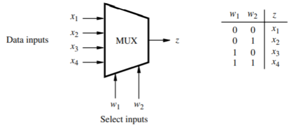
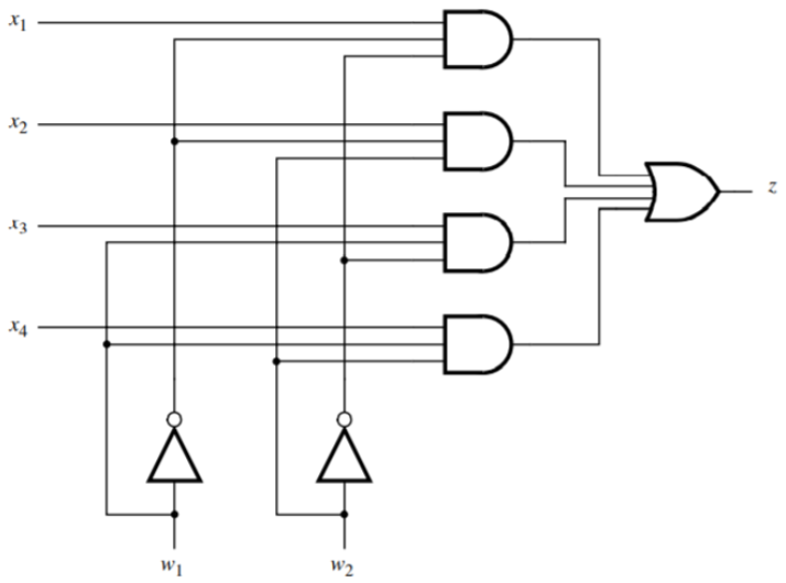
- The decoder on the other hand only has selection inputs, i.e. n, and at and at most (and generally close to) \(2^n\) outputs.
- The decoder is like if a multiplexer had all selection inputs to be high and the last XOR get gets removed and replaced by each of the incoming signals into separate output pins, of which all but one will be low.
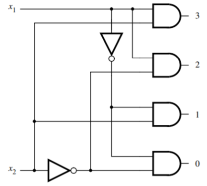
- To build a decoder follow these 3 steps
- Provide a selection pin for each address bit and immedeately breanch out it’s inverse
- Build the output AND gates based on binary order:
- Smallest address has all inverted pins (0s), biggest address has all non-inverted pins (1s)
- Fill the gap and map the inverted and non-inverted pins with the relevant AND gates
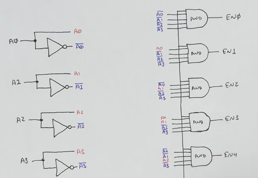
- The additional variable of the AND gates is reserved to the ENABLE signal (not shown in the picture) such that to enable a memory address we just need to provide the address signals and the enable signal
- To build a multiplexer you follow the same steps but on each AND gate you add a unique data input and then you XOR all the AND gates into one output signal
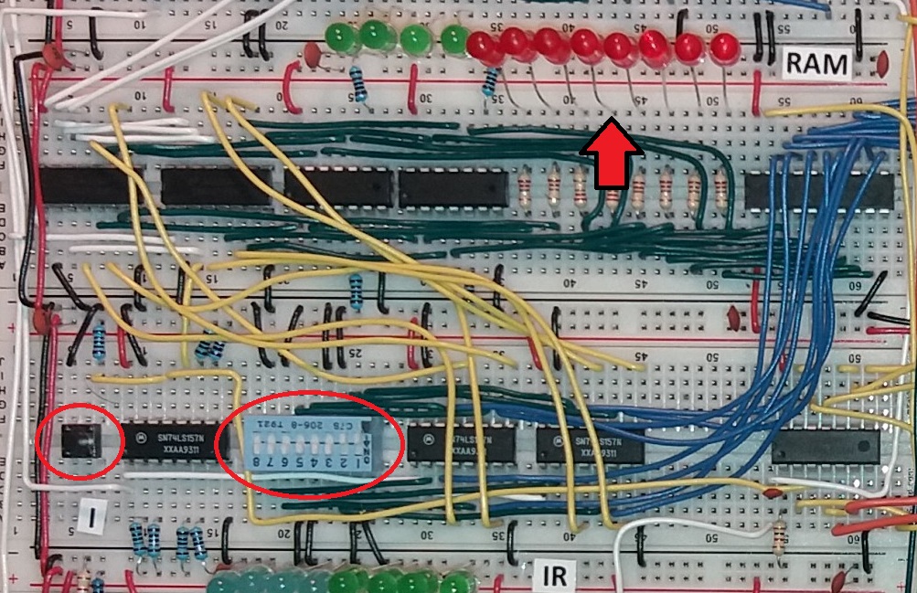
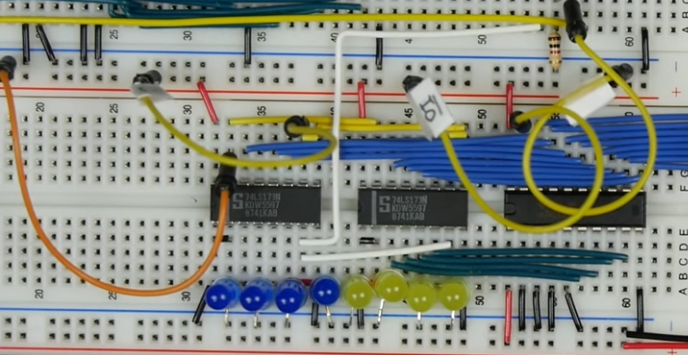
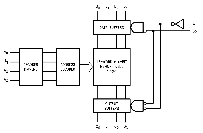
74LS189 (16 4-word address RAM)
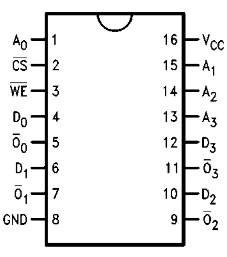
- 64 bit random access memory
- This static RAM holds 16 4-bit words
- There are 4 An pins to address one of the 16 words (it includes an address decoder)
- We can hookup the address pins of 2 74189 4-bit word RAMs such that they share the same address signals and one chip stores the 4 MSB and the other one the 4 LSB making it a 8-bit word x 16 addresses RAM (16 byte RAM)
- The data inputs are Dn
- Output inputs are \(\overline{O_n}\), indeed they are inverted
- The outputs are active only in the Read mode, therefore while \(\overline{WE}\) is low the output LEDS might behave weirdly
- WE = write enable (loads data from the input pins and saves it to the memory given to the address pins), the pin is inverted.
- CS = chip select (enable to Bus)
- The pin is also inverted, so we will connect it to ground (such that it is always enabled so we can hookup LEDs and see its contents) and connect it to a tri-state buffer like we did with the registers. If we don’t want to hookup LEDs to the RAM, we can just use the tri-state output logic that the chip itself includes:
- \(\overline{CS}\) low & \(\overline{WE}\) low = Write
- \(\overline{CS}\) low & \(\overline{WE}\) high = Read
- \(\overline{CS}\) high = disconnect output to Bus
- I’m assuming that the inputs don’t need a tri-state buffer and can be connected all the time to the Bus since they don’t sink that much current anyway as input pins usually have around ten mega ohms of resistance.
- This part is covered here
- This part is covered here
- The pin is also inverted, so we will connect it to ground (such that it is always enabled so we can hookup LEDs and see its contents) and connect it to a tri-state buffer like we did with the registers. If we don’t want to hookup LEDs to the RAM, we can just use the tri-state output logic that the chip itself includes:
- The chip that came in the kit did not have “LS” family explcitily written and it seemed to get pretty hot during some tests with floating pins. Therefore make sure to not leave floating pins and those that are high should and be connected to \(V_{cc}\) should be with a \(1k\Omega\) pull-up resistor.
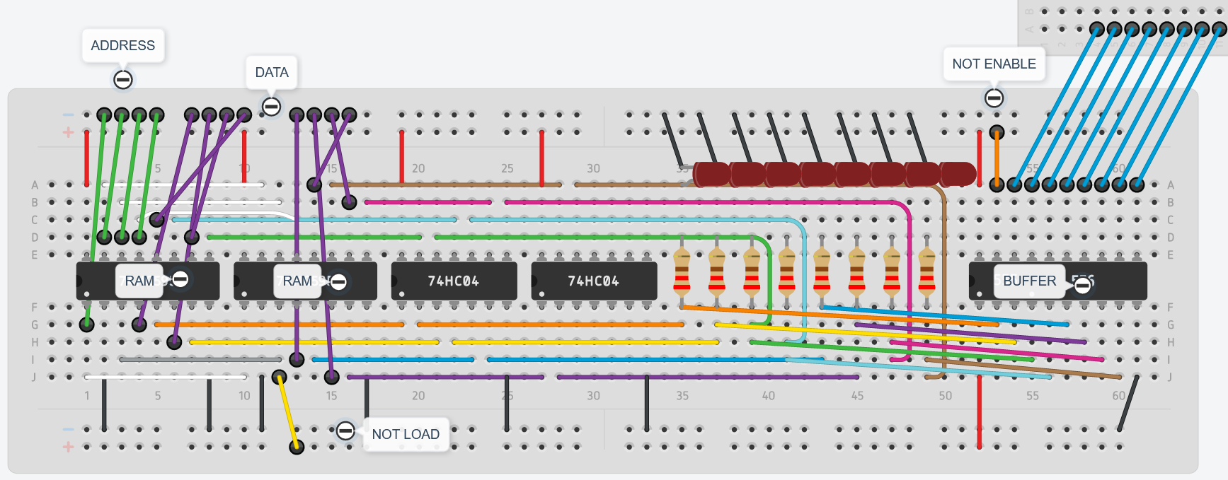
Building the RAM
- Insert chips 2 74LS189 and 2 74LS04 inverters on the breadboard and hookup the power and ground pins
- Hookup outputs of the RAM to the inverter inputs
- Hook up resistors and LEDS to the inverted-inverted outputs
- Hook up \(\overline{CS}\) to ground on both RAMS
- Insert 3-state buffer (74LS245) and connect power, ground and dir (to \(V_{cc}\)) pins
- Connect inverted-inverted outputs to the tri-state bottom pins
- Connect same address pins together from both RAMs
- Then use a jumper wire for each grouped address pin and connect it to ground as a temporary signal cable
- Connect jumper wires to each data pin as a temporary signal (later it will be connected to the DIP switches rather than to the Bus)
- Connect both \(\overline{WE}\) pins together and a jumper wire to use it as temporary signal
Tinkercad
 Open tinkercad
Building the memory address register (and a “programming mode” version)
- The jumper wires for the address will be connected to the outputs of the memory address register, the register that contains the current location of the RAM we’ve readily available to use
- Remove the power rails of a new breadboard and fit it between the clock breadboard and the RAM breadboard
- We’ll use a single 74LS173A (4 bit register) for the memory address register
- This register will be connected to the Bus, as we expect the computer on “running” mode to share memory addresses via the Bus, and store that value there
- The outputs of this register will be connected (via a multiplexer) to the RAM address pins
- The multiplexer would allow to chose between the memory address register and a manual switch to feed the RAM address pins
- The reason we don’t connect the Bus directly to the address pins of the RAM is that the bus can only hold 8 bits of information and if we wanted to write something on a given memory address we’d just have lost 4 bits to determine the address and thus 4 information bits to write are gonna be truncated
- Just reading the contents of a RAM address by just relying on the Bus to get the address is pin feed is problematic too as in that same clock pulse the Bus is supposed to hold the RAM address then whoever outputed that to the Bus must disable its outputs and to allow the RAM at the address specified by the Bus to output its contents. Thus getting the address and outputting the contents to the Bus just right as the other module disables its Bus output looks very complicated to implement in a reliable way, therefore we use the address register to store which ever address we need to use.
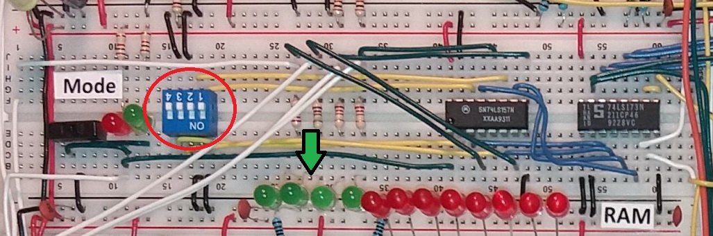
- We use a 4-bit DIP switch as the “programming mode” alternative to feed the address pins of the RAM (via the multiplexer)
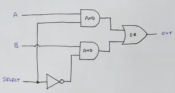
- The multiplexer logic to select between 1 bit of register address (run mode or “A”) and 1 bit of manual address (programming mode or “B”) can be described by the logic circuit below.
- The 74LS157 does that for us, and it has four 2-data/1-selection pins multiplexers
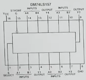
- The strobe pin is just an additional (inverted) control input to all AND gates, we just hook it up to ground to make the chip behave as the previosly shown multiplexer logic circuit.
- The 74LS157 does that for us, and it has four 2-data/1-selection pins multiplexers
- Implementation steps:
- Insert the DIP switch, the 74LS157 multiplexer (mux) and the 74LS173 register.
- Set power and ground pins
- Set strobe to low (mux)
- Output control (pins 1 and 2 of register, which you have to merge) to low as well (we want to always see the lights
- Connect pins 9 and 10 (not load) and a jumperwire cable to use it as a temporary signal
- Connect register clear to ground
- Connect clock pin to the clock
- Connect the outputs of the register to the B inputs of the mux
- Connect one end of the DIP switches to the A inputs of the mux, the other end to ground.
- We’ll be utilizing the fact that the default value of floating pins for the 74LS157 mux is high, therefore we alternate between ground and floating (high)
- Connect a slideswitch with common (midle pin) to ground (this is best practice), and the 2 terminals to \(V_{cc}\), each with a \(1k\Omega\) resistor and a LED
- Then the slideswitch determines which of the terminal gets to be connected to ground and thus has 0V, while the non-selected terminal has the voltage it’d have as if the slideswitch didn’t exist.
- Connect one of the terminals to the select pin of the mux, such that the terminal that you chose matches the LED pattern that you want. When the LED is shining, it actually means that the voltage of that terminal is 0V (the terminal is grounded and no more current will flow to any other branch other than back to the power source, had it not be grounded, then the votlage would have been high)
- The datasheet of the 74LS157 shows that the select pin is inverted, so a lighting LED terminal (with 0V) is eventually a high select, which then selects A inputs (DIP switch). Therefore programming mode will be equal to the (lighting) LED whose terminal is connected to the select pin of the mux (pin 1)
- Connect the outputs of the 74LS157 to 4 address LEDs (with 220 resistors)
- Connect the outputs of the 74LS157 to the RAM address pins
Tinkercad
 Open tinkercad
Schematic
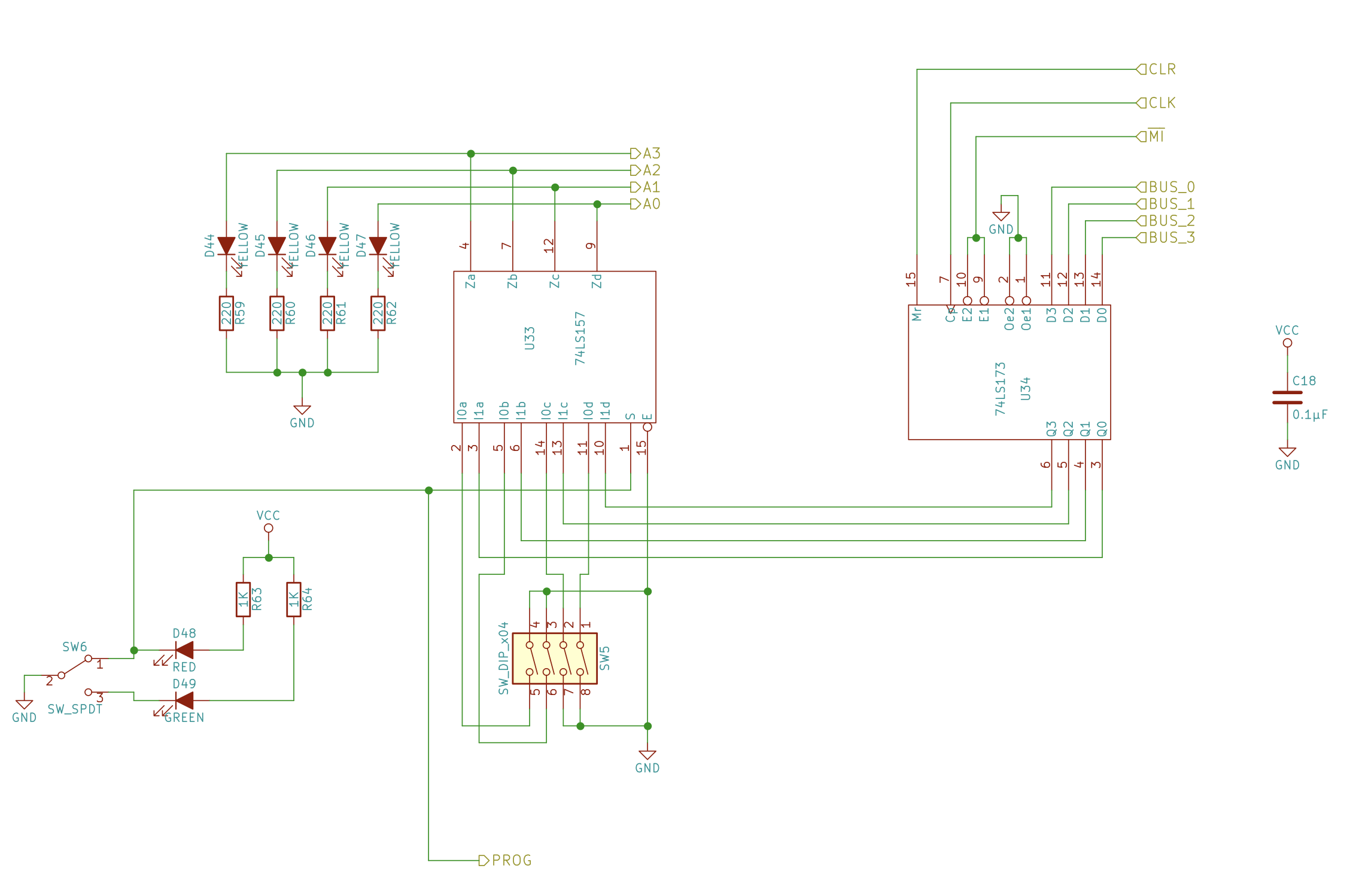
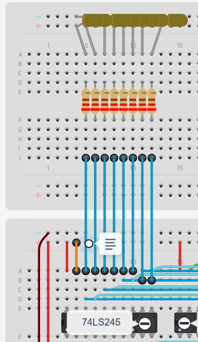
Building an 8-bit input terminal for the RAM (to manually store a program) and the alternative of inputs from the Bus
- We’ll stick a breadboard under the RAM module and above the instruction register
- We’ll use the same signal for “programming mode”/”running mode” that the address register mux uses for the input mux, where A inputs come from the 8 bit DIP switch and the B inputs come from the Bus.
- For 8 bits we need to deploy two mux chips (74LS157)
- Building steps:
- Insert the 8 bit DIP switch and the 2 mux
- Hookup power and ground pins, and both strobes of the multiplexers (pin 15) to low
- Connect one of the DIP terminals to the mux A inputs (Big Endian, MSB goes to A1, pin 2), the other terminal to ground (because then the bit is either grounded (low) or floating (high in LS chips))
- We did BIG endian for the address (most significant bit was output 1 of the MUX, pin 4), so we’re gonna do BIG endian with the data pins too.
- Connect A inputs to the bus (Big Endian)
- Connect the outputs of the mux into the data pins of the RAM (Big Endian)
- Tie both select pins (1) of both data muxes together
- Replace the RAM “Not Load” signal (\(\overline{WE}\)) with the output of yet another mux
- Tie this mux select to both, the programming/run mode switch signal and the select pin of the 2 data multiplexers.
- The purpose of this mux is to provide the adequate write signal to the RAM depending on which mode we are (programing or run):
- Manual pushbutton (for programming mode)
- Clock pulse and “instruction signal” (for run mode)
- Manual pushbutton:
- Insert DIP push button and mux chip next to each other
- Connect power/ground pins, then strobe to ground
- Connect one of the outputs, i.e. output Y4, to the \(\overline{WE}\) pin of the RAM
- Connect one pushbutton terminal to the ground and the other one to the A4 input of the mux
- Control logic (clock):
- We don’t want to let the control logic trigger an immediate write signal, we want to synchronise that write signal for the next clock cycle, therefore we’ll use a NAND gate (\(\overline{WE}\)) is inverted tha’ts why we use a NAND gate so that the output is also negated) that takes two signals, the clock pulse and logic signal from “control word”. Therefore, insert the NAND gate on the breadboard.
- Hookup the power/ground pins of the NAND gate
- Connect the output Y1 of the NAND gate to the B4 input pin
- Connect the input B1 of the NAND gate to ground/\(V_{cc}\) via a jumperwire that we will use as a temporary signal until we build “Control world”
- Now this write signal is no longer inverted and a high signal means write, low signal means not write.
- Connect input A1 of the NAND gate to the following edge detector circuit:
- Connect \(1k\Omega\) resistor from ground to pin 1
- Connect one leg of a \(0.01\mu F\) capacitor to the resistor (basically to pin 1)
- Connect the other leg of the capacitor to the CLOCK signal
Tinkercad
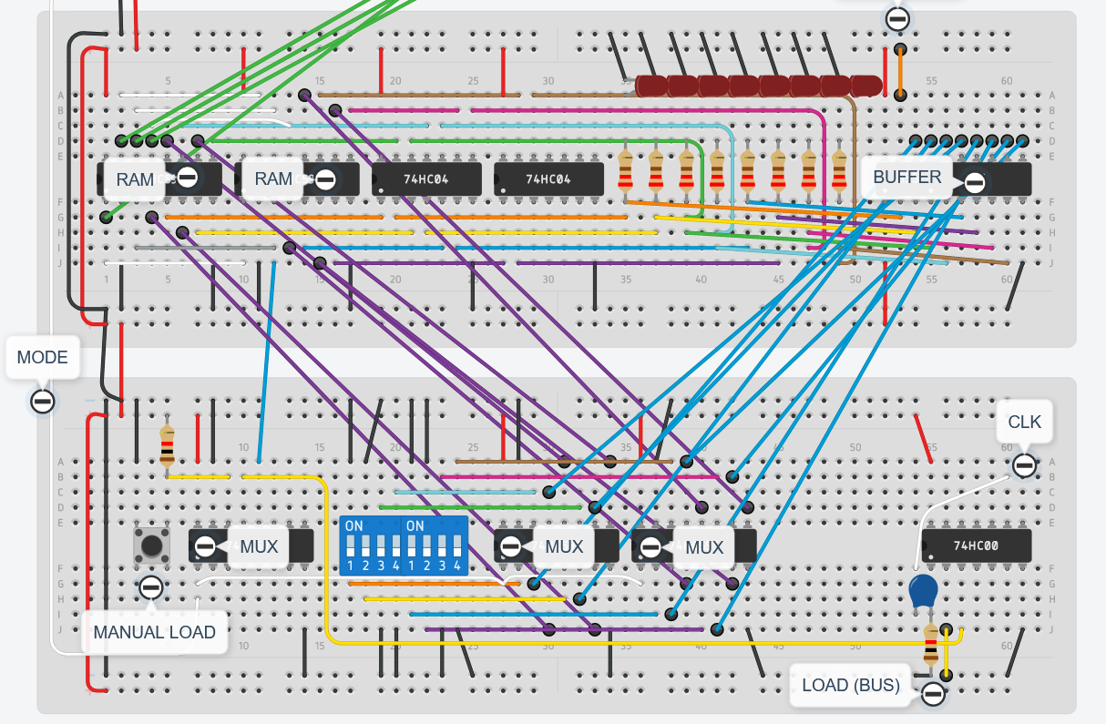 Open tinkercad
Schematic
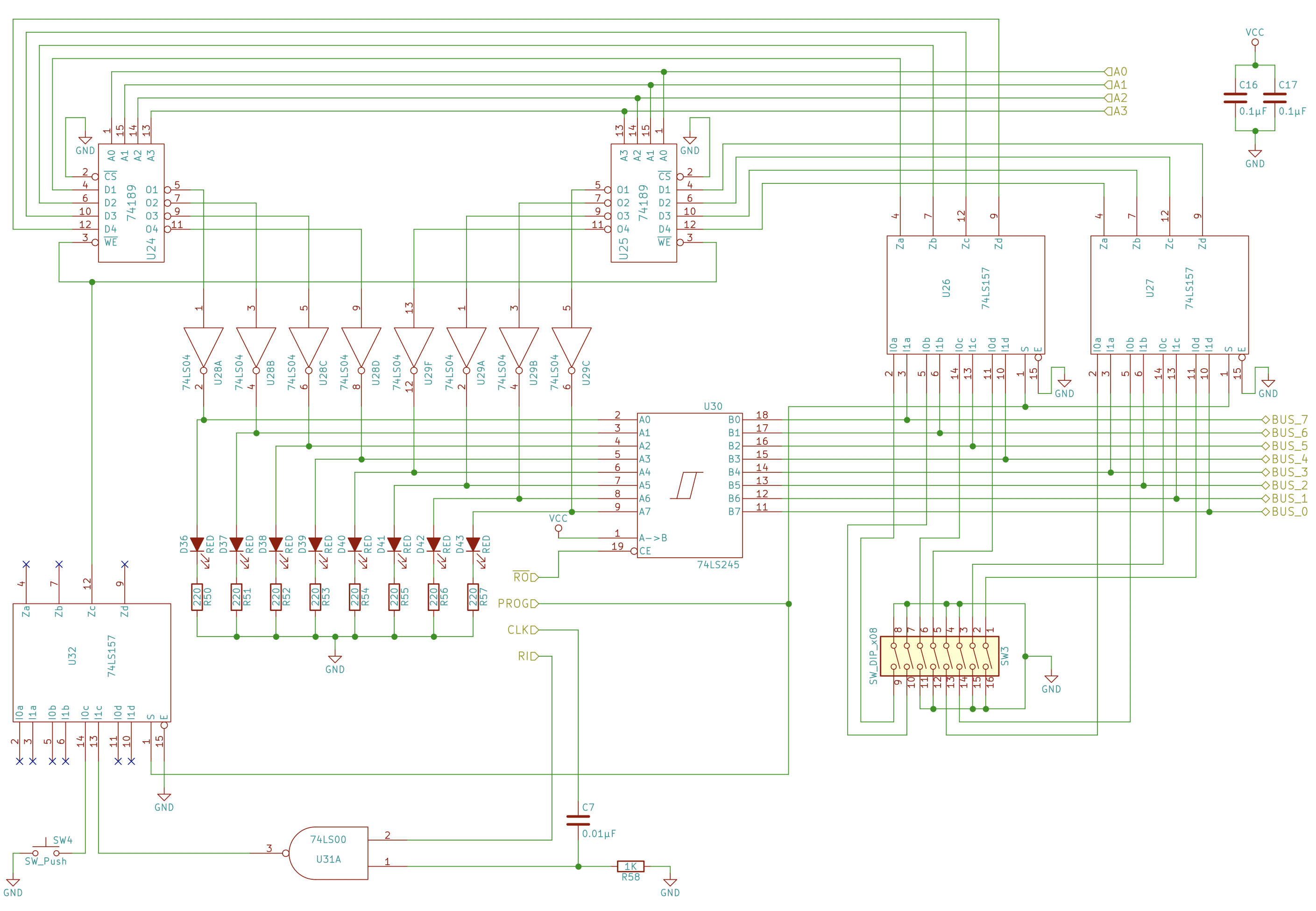
Testing the RAM
- Floating inputs from the bus to the mux B inputs for storing data on the RAM behave randomly and not as expected (float = high)
- While you mantain the push button to write data manually the LEDs behave weirdly as earlier observed, therefore it might be better to press the button quickly and not hold it for too long.
- If the capacitor at the ram input module affects the clock signal to the rest of the circuit (especially to the program counter if the capacitor discharges via the clock signal ), instead of having a resistor + capacitor circuit for the clock signal, let the inputs of the NAND gate be the unaltered clock signal and the logic signal and then create a resistor + capacitor circuit for the output of the NAND gate, and then feed that signal to the multiplexer (this should work well as the resistance of the output pin is much higher than the pull-down resistor and the capacitor should be fully discharged via the resistor)
- However the capacitor should take \(0.01\mu F \cdot 1k\Omega = 10\mu s\) to charge (so a 10 microseconds pulse), and then it should discharge via the resistor while the clock signal is still high (so it’s very unlikely that current will want to discharge in the direction where high voltage is coming from)
Labeling jumperwires (control signals) and architecture overview
- At this point of the project we have reached a large number of signals, and some of these are regarded by the pin name given by the manufacturer while others have been nicknamed by it’s purpose.
- While these names were clear within the context of their modules, they need to be better differentiated when looking at all of the signals from the bigger picture.
- We’ll provide the final version of the control signal names, which will later be used to develop our own machine code.
Architecture
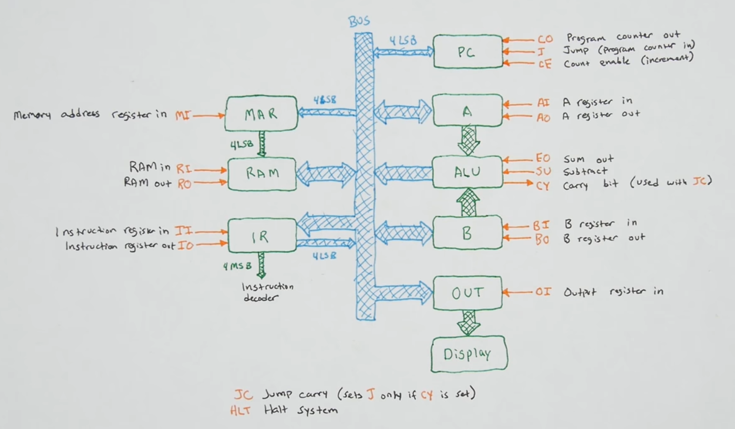
- Disclaimer: The program counter, output & display, and the instruction decoder have not been implemented yet
Control signals
- Special note: “Not” means that the signal is inverted
- These signals are formally regarded as “active low”
- \(HLT\) = halt (makes low) clock signal = the last input of the last AND gate of the clock logic circuit.
- Reminder that the inverter is not implemented and thus HLT is active low (which is the opposite Ben Eater has)
- \(\overline{MI}\) = Not Memory address register in = “Not load” signal of the memory address register
- \(\overline{RO}\) = Not RAM out = “Not enable” signal of the RAM’s tri-state buffer that controls whether to output to the content of the RAM (at the address pointed by the memory address register/DIP switch) to the Bus or not.
- \(RI\) = RAM in = “Load (Bus)” input signal of the NAND gate in the RAM input module that takes the pulse detector circuit as other input and feeds it to the programming mode/run mode multiplexed signal for the RAM’s \(\overline{Write\ Enable}\) pin.
- Since the NAND chip inverts the output, the signal is active high.
- \(\overline{IO}\) = Not instruction register out = “Not enable” signal of the instruction register tri-state buffer (located on the right, mirroring the design of the A & B registers with respect to the Bus) to output the bus.
- \(\overline{II}\) = Not instruction register in = “Not load” signal of the instruction register to save the inputs (from the bus) into the instruction register.
- \(\overline{AO}\) = Not register A out = “Not enable” signal of register’s A tri-state buffer that controls outputting to the Bus.
- \(\overline{AI}\) = Not register A in = “Not load” signal of register A pin to store the inputs (from the Bus, who is always listening)
- \(\overline{BO}\) = Not register B out = “Not enable” signal of register’s B tri-state buffer that controls outputting to the Bus.
- \(\overline{BI}\) = Not register B in = “Not load” signal of register B pin to store the inputs (from the Bus, who is always listening)
- \(\overline{EO}\) = Not ALU’s \(\Sigma\) (operation outcome) out = “Not enable” signal of ALU’s tri-state buffer that controls outputting to the Bus.
- \(SU\) = Substract = ALU’s active high signal to make the operation be A-B instead of A+B when it’s low
- \(CE\) = Count Enable = Enable pins of the 4-bit counter = Allow the counter to increment by 1 at each clock pulse
- \(\overline{CO}\) = Counter out = active low enable signal of the output tri-state buffer of the counter that determines whether the outputs are sent to the Bus or are disconnected.
- \(\overline{J}\) = jump = active low load signal of the 4-bit counter to store the contents from the inputs (Bus)
Testing RAM with Registers and ALU
- I started to put the modules I have into the final layout, with a Bus line in the middle. For the Bus line I used jumperwires for the RAM and register B and hookup wire for register A, the ALU, and the Bus lights (yep, I decided to placed them on the below the instruction register breadboard as it had some available space and I did not have soldering equipment as Ben did). Everything seems to work fine except for the following bugs
- In programing mode, if you have \(\overline{RO}\) low and either \(\overline{AI}\) or \(\overline{BI}\) and you manually change a value in the RAM, the contents of the register are sometimes changed with random values.
- Workaround: don’t have registers loading from the Bus while you’re saving inputs into the RAM
- Origin: the bug might be linked to the weird behavour of the outputs of the RAM when they RAM inputs are being saved. This might affect the Bus and the registers connected to it. So take the workaround as a safety guideline until the bug is fixed.
- Solution: Power/ground rail connection between clock and counter module seems to fix this problem
- In running mode both registers and RAM, when they load something from the Bus, they don’t load the default 00000000 but random values if there’s nobody outputting to the Bus.
- Workaround: do not rely on the Bus being 0000000 if nobody is outputting
- It seems to greatly reduce the probability of not saving all zeros when you connect the bottom power/ground rail the clock module and the counter module. It will occasionally give a random value.
- In programing mode, if you have \(\overline{RO}\) low and either \(\overline{AI}\) or \(\overline{BI}\) and you manually change a value in the RAM, the contents of the register are sometimes changed with random values.
- In run mode as long as there is 1 party outputting to the bus you can have register A and RAM both loading the Bus at the same time without problems.
- The ALU doesn’t seem to work well when the clock speed is too fast
- When I removed the jumperwires of the RAM that I was no longer using and the pulldown resistors of the Bus it seemed to work perfectly.
- Decision: replaced remaining jumperwires with hookup wires and test the same scenarios with and without 10k resistors
- If it doesnt work wth 10k but it works withou resistors try to replace the 10k resistors with 1k resistors
- Another solution for the potential problem of the capacitor travelling back the clock signal to the PC is to insert a LED in between that forces the current to only go in the desired direction (from the clock module to the RAM input module only)
- Tried it, and it turns out to drop too much voltage and the RAM doesnt write at all
- Final solution:
- I put the clock signal for the RC circuit (resistor capacitor edge detector circuit) into the inverter chip of the clock module, then put the output again in the inverter and used the second inversion (double negation cancels out) into the RC circuit, which now no longer creates double clock pulse to the reigsters and ALU.
- The reason I did it was because the previous attempt at preventing the RC circuit from feeding current back to the clock signal (and hence to the other modules and disrupting the clock cycles) using a LED (a diode, which forces current to go one way only) was unsuccessful as the LED seemed to drop too much voltage and the RAM couldn’t write anything at all (here I’m assuming that the reason it didn’t write was because the voltage to the mux input was too low, did not have equipment to assert it). Luckily the inverter outputs seem to include diodes as the datasheet sugested, and the output pin allowed a voltage from 0 up to \(V_{cc}\), so I did not have to worry about the capacitor damaging the inverter, apparently the diodes of chip had a smaller voltage drop than the yellow LED I used.
- \(\overline{MI}\) shares the same signal with the RC circuit, but I don’t care if \(\overline{MI}\) get’s double clock pulses, (it just saves the same thing twice), as it does not cause any harm and breadboard real estate is expensive.
- I’ve also trimed the power supply cables as they were a bit burnt in the top, I might have accidentally removed them from the breadboard before disconnecting the power supply and I might have shortcircuit them. This could have created resistance and limit the power supplied to the breadboards
- At this stage, I haven’t repalced the RAM tri-state buffer jumperwires for hookupuwires, so the RAM loads random values when nobody is outputting to the Bus, but both registers A and B seem to load 00000000 default values, so whether using hookup wires for the RAM buffer fixes the issue or not is not a big deal since we can work around this issue by loading the registers first, then moving that value to the RAM.
- The problem of the RAM writting things at random times on programming mode without pressing the button is because Ben’s default schematic leaves the input floating when the button is unpushed, hoping that the active low pin will recognise the floating input as high, but since power is not reliable is better not to have it as a floating input and use a pull-up resistor instead, a 1k should do the trick.
- In hindishgt, the issues seemed to be power bugs
- I put the clock signal for the RC circuit (resistor capacitor edge detector circuit) into the inverter chip of the clock module, then put the output again in the inverter and used the second inversion (double negation cancels out) into the RC circuit, which now no longer creates double clock pulse to the reigsters and ALU.
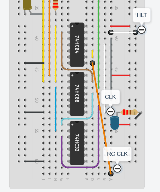
- This doesnt fix the problem when inserting manual data to the RAM and having a register listening to the Bus, which regardless receiving not clock pulse, writes some garbage (so always disconnect registers from the Bus when writting manual input into the RAM)
- Apparently got fixed after replacing jumperwires with hookup wires and moving the Bus leds and pull-down resistors to the bottom of the computer
- I have also also decided to invert HLT and make it active high like Ben, it may make the instruction decoder easier if I have the same signals as him.
- After replacing the jumperwires with hookup wires everything seems to work fine besides writing to the RAM
- Loading an empty bus gives random values for the RAM only (registers A and B seem to store all 0’s)
- However, if both A and B are listening, then only one gets all 0’s and the other gets all 1’s. Seems that all the current sinks through the input pins of one register and the other register input pins can only interpret an open circuit. Perhaps the 10k ohm resistors don’t sink enough current for the RAM to recognise the low voltage?
- Even if you are in programing mode, if you leave the \(RI\) signal high every 100th pulse of so it will write the contents of the DIPs without pressing the button
- I dont think the \(RI\) signal itself has nothing to do, but rather the fact that the logic behind the push button is that Write Enable of the RAM is active low, the button either connects the pin to ground or leaves it floating.
- Since the breadboard computer has gotten very large, the powerrails might have quite some noise and floating inputs are no longer reliable.
- Luckily we only use the floating inputs for manual logic. Therefore this bug will be ignored until it causes larger problems.
- Loading an empty bus gives random values for the RAM only (registers A and B seem to store all 0’s)
Program counter (PC)
- The programs that we run are stored in the RAM
- We have a maximum of 16 addresses that contain 1 byte of data each
- In each of those bytes we store a set of instructions in binary
- Our programs first instruction will start at address 0
- And unless a jump or conditional is faced, the program will generally move to the next address
- In order to execute any instruction, we have to do the fetching process to extract that info from the RAM
- That RAM info is moved from RAM to the instruction register
- We use a program counter to keep track of which (instruction/program) address we’re on
- In many ways the program counter works as register
- stores a value
- can put it on the bus
- can load a value from the bus
- However the value of the program counter register has a very specific meaning, which is the address of the next instruction we’re gonna execute
- The control logic signals of the program counter are:
- CO = (Program) counter out = put stored value on the Bus.
- J = jump = essentialy load the value (4 least significant bits) in the Bus like any other “in” signal.
- CE = Count Enable = increment the counter
- We do not want to increase the program counter (which points to the the next address that we will execute) at every clock cycle but at the eand of each whole programmed instruction (as those take a couple of clock cycles to complete) (it still need to be synchronized with the clock nevertheless)
- In many ways the program counter works as register
- Sections below introduce the the logic behind a program counter and it’s implementation in our computer
JK flip-flops
- It’s an upgraded version of a SR flip-flop
- Enable signal replaced by a clock edge circuit (clock signal + capacitor + resitor circuit), hence “flip-flop”
- Furthermore, the outputs are fed back into the AND gates such that it produces the following truth table
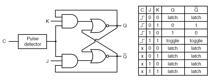
- Not only gets rid of the unpredictable (and hence illegal) 11 state, but also makes it an interesting feature, to output the opposite value it previously had (toggle)
JK flip-flop racing
- It happens that in a regular JK flip-flop, the clock pulse is actually long enough such that if we set JK to 11 (toggle), the outputs will toggle continously during the whole duration of the pulse, which may not necesarily be consistently long and hence sometimes having an odd number of toggles and other times an even number of toggles, leaving us with an impredictable result after all
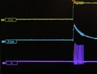
Master-slave JK flip-flop
- Gets rid of the racing problem
- Trying to get a very short clock pulse such that there’s not enough time for the output to race back into the AND gate with a now low clock signal is almost impossible to do with reliably with breadboards, instead we use 2 JK flip-flops together in the following way:
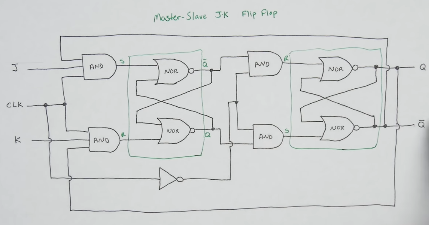
- We no longer need a pulse signal, just the clock signal.
- We can identify some sort of 2 SR latches inside the circuit
- The first (left) SR latch will not be high unless the clock is high, whereas the second one (right) would be active while the first SR latch is not, as it uses an inverted clock signal.
- Therefore we will never have an scenario where both SR latches are active.
- To pass a value (set or reset) to the second latch (right one, the one that eventually has the Q and \(\overline{Q}\) outputs), we first need to pass it to the first latch and wait till the clock is high, then once is stored in the first latch we have to wait for the clock signal to get to low such that the second SR becomes active. This works well for all combinatons of J and K, including JK = 11, as the racing problem doesn’t occur since when the second SR latch is active and has fliped Q, it doesnt matter how fast Q races back to the first SR latch because that one is inactive until the clock rises anyway.
- Therefore JK = 11 with a master-slave toggles Q at each clock cycle
74LS76
- IC implementation of 2 indepedent master-slave JK flip-flops
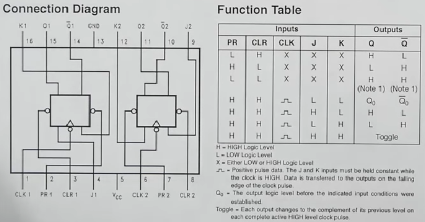
- PR and CLR bypasses the clock signal and it forces either a 1 or a 0.
- The buble before the clock signal indicates that the masterslave indeeds is triggered at the falling edge of the clock
Binary counter
- One JK master-slave flip-flop feeding its clock signal from the clock, with JK = 11, toggles at every (falling edge) of a high clock
- The toggle means that half of the times we have high output, the other half we have low output.
- So for every 2 high clocks, we just had 1 high output
- This is called a “divide by 2” circuit
- We can hookup another JK master-slave flip flop, whose clock signal is ANDed with the output signal of the previously mentioned JK master-slave flip-flop, which we can interpret as being the least significant bit.
- This n bit will toggle every \(2^n\) clock pulses, with n being the bit it represents.
- This means it will be \(2^{-(n+1)}\) as fast as the clock pulse
- By connecting more master-slaves in this fashion we can create a simple binary counter.
- Example of a counter with the 74LS76
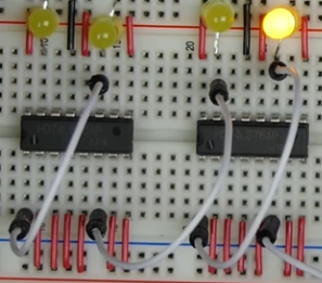
- Example of a counter with the 74LS76
74LS161
- This IC is a synchronous (uses the clock) 4-bit binary counter implemented in a similar way as the counter we described earlier, but with some other features:
- The clock pin is inverted such that now the counter is triggered at the rising edge of the clock like in all other modules pulse logic.
- It comes with data pins that allows us to easily load a value in the next clock pulse
- It comes with an enable input that can let continue or freeze the counter
- Ripple carry out is to cascade more counters into larger bit counters and clear is to set it to 0
Building the program counter
- Place breadboard on top of the A register
- Place one 74LS161 (4-bit binary counter) and a tri-state buffer (74LS245) to its left (close to the Bus).
- Hook up power and ground pins for both chips.
- Set the DIR pin low of the tri-state buffer (we always use the buffer one way only, namely to output stuff)
- This time we will use B->A direction because of the location of the output pins of the counter chip (above)
- Use a jumperwire signal for pin 19 of the tri-state buffer (\(\overline{E}\)) with the label “\(\overline{CO}\)”
- Connect MSB of the output buffer (B1, B2, B3, B4) to ground
- Connect the output bits of the 4-bit counter (little endian) to the 4 least significant B pins of the tri-state buffer (big endian)
- \((Q_A, B8), (Q_B, B7), (Q_C, B6), (Q_D, B5)\)
- Connect the outputs to green LEDs with 220 ohms resistors
- Pin 9 (LOAD) is for the “JUMP” jumperwire signal, which the circle of the diagram indicates that is inverted (so add lable “\(\overline{J}\)”), which basically stores the inputs into the counter.
- \(CE\) jumperwire signal is acheived by connecting pins 7 and 10 and from there the jumperwire (active high).
- Connect the clock signal (the normal one, not the one for the RC circuit) to pin 2
- Connect the 4 least significant A pins of the tri-state buffer (big endian) to the inputs of 4-bit counter (little endian)
- \((A, A8), (B, A7), (C, A6), (D, A5)\)
- Connect all A pins of the tri-state buffer to the Bus.
- Set the clear pin of the counter to high as that one is active low
Tinkercad
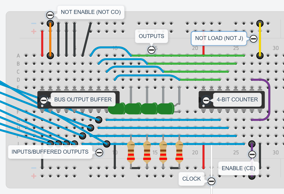
Schematic
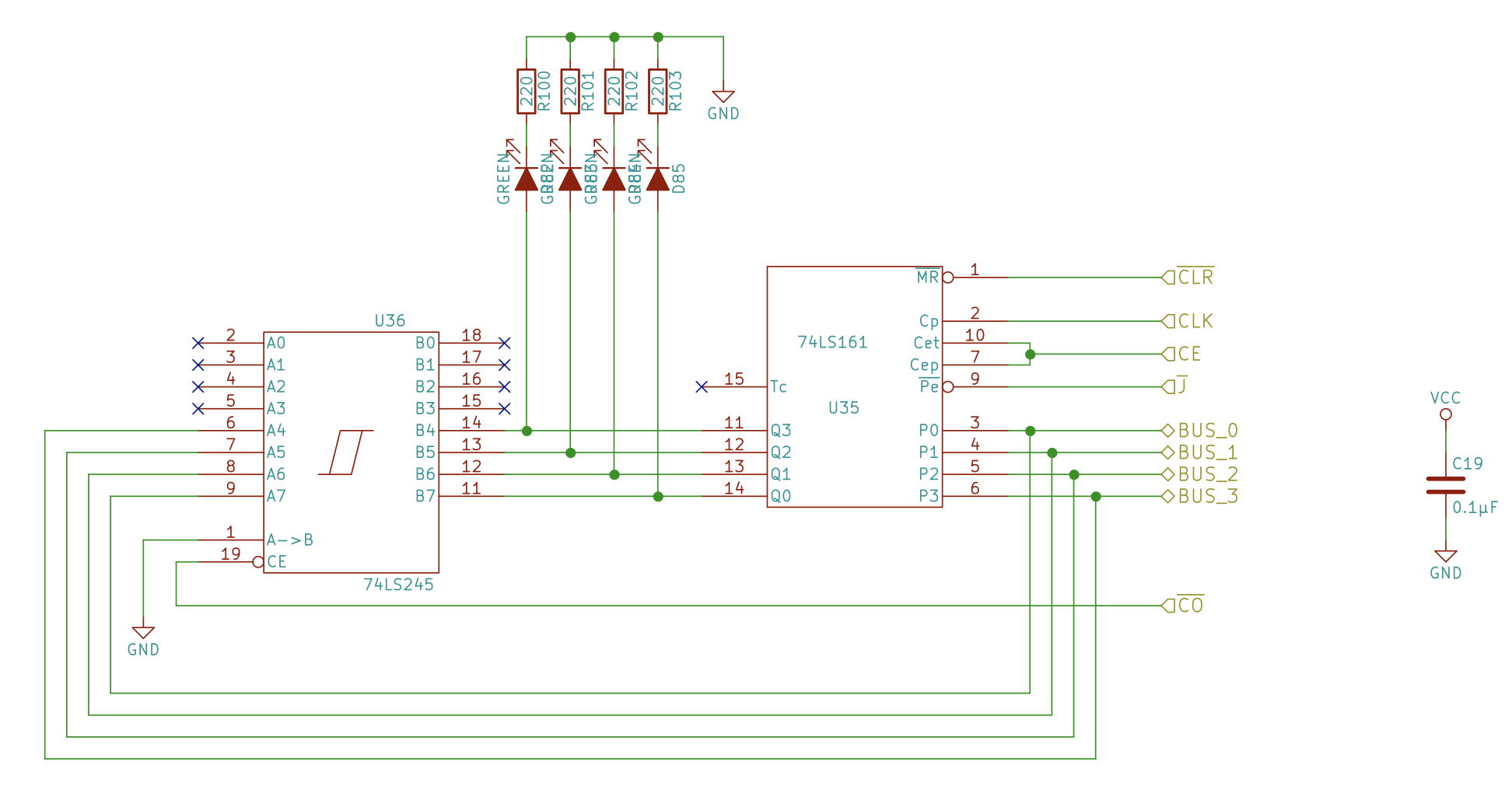
Testing the program counter
- Reading test: do the i++ ALU test
- Writting test: Load contents to another register/RAM in combination with CE (counter enable) high
Output module
- Components in the kit (including control logic):
- 6 breabdoards
- 1 Arduino Nano
- 1 555 timer
- 1 74LS00 Quad NAND gate
- 1 74LS02 Quad NOR gate
- 2 74LS04 Hex inverters
- 2 74LS08 Quad AND gates
- 1 74LS107 Dual J-k flip-flops
- Ben’s videos use the 74LS76, it has the same functionality but different pins! So checkout the datasheet
- 3 28C16 EEPROMs
- 1 74LS138 3-8 line decoder
- 1 74LS139 2-4 line decoder
- 1 74LS161 4-bit counter
- 1 74LS173 4-bit D register
- 1 74LS273 8-bit D register
- 2 74HC595 8-bit shift register
- 1 Momentary pushbutton
- 1 Slide switch
- 40 \(220\Omega\) resistors
- 5 \(1k\Omega\) resistors
- 10 \(10k\Omega\) resistors
- 5 \(100k\Omega\) resistors
- 20 Red LEDs
- 10 Green LEDs
- 4 7-segment LED display (LTS547R)
- 5 \(0.01\mu F\) capacitors (103)
- 5 \(0.1\mu F\) capacitors (104)
- The output reigser is similar to any other register, but we want it to have a (7-segment) decimal display.
LTS547R (Jameco 7-segment LED display)
- Red
- Common cathode
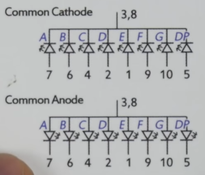
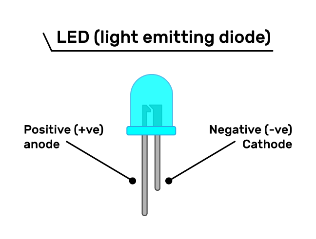
- Maximum Forward Voltage: 1.6 V (@ 20 mA)
- Maximum forward current: 20mA
- We need a series resistor to limit the current.
- \(V=IR\)
- \(5V = 0.02 A \cdot R\)
- \(R = \frac{5V}{0.02A} = 250 \Omega\)
- Two \(220\Omega\) resistors should do the trick
- \(I = \frac{V}{R} = \frac{5}{440} = 11.36 mA\)
- Less than half the maximum current, it should light it up enough.
7-segment hex decoder
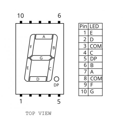
- Below a common cathode representation for 4 bits
- A common annode would just be “off” (20 amps to ground) instead of “on” (20 amps from \(V_{cc}\))
| Binary | Digit | Display | a (7) | b (6) | c (4) | d (2) | e (1) | f (9) | g (10) |
|---|---|---|---|---|---|---|---|---|---|
| 0000 | 0 |  |
on | on | on | on | on | on | |
| 0001 | 1 |  |
on | on | |||||
| 0010 | 2 |  |
on | on | on | on | on | ||
| 0011 | 3 |  |
on | on | on | on | on | ||
| 0100 | 4 |  |
on | on | on | on | |||
| 0101 | 5 |  |
on | on | on | on | on | ||
| 0110 | 6 |  |
on | on | on | on | on | on | |
| 0111 | 7 |  |
on | on | on | ||||
| 1000 | 8 |  |
on | on | on | on | on | on | on |
| 1001 | 9 |  |
on | on | on | on | on | on | |
| 1010 | A |  |
on | on | on | on | on | on | |
| 1011 | B |  |
on | on | on | on | on | ||
| 1100 | C |  |
on | on | on | on | |||
| 1101 | D |  |
on | on | on | on | on | ||
| 1110 | E |  |
on | on | on | on | on | ||
| 1111 | F |  |
on | on | on | on |
Karnaugh maps
- We could implement a decoder logic circuit with the same style as described in the address decoder section (which made sense since we were using all 16 addresses from those 4 bit combinations). Or we could just focus on one segment at a time and simplify it’s truth table with a karnaugh map (a technique to simplify boolean expressions), since we just want to use 16 “addresses” (7 segment display representation) out of the \(2^7=128\) possible representations.
- If we name the 4 bit inputs A, B, C and D, you’ll see that sometimes instead of writting \(\overline{A}\overline{B}\overline{C}\overline{D}\) and \(ABCD\) we will just write the decimal version of 0000 and 1111 respectively i.e. \(\overline{A}B\overline{C}D\) is 5
- Karnaugh map for segment “a”
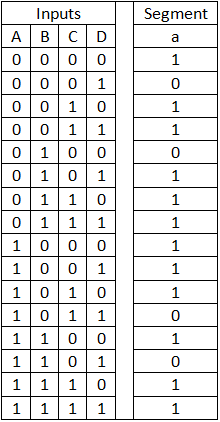
- The truth table can be expressed as a single boolean expression by “ORing” each row with “a” equal to 1. So “a” will be true/high/on If we have 0,2,3,5,6,7,8,9,10,12,14, or 15
- The karnaugh map simplifies this expression from 12 terms to 6!
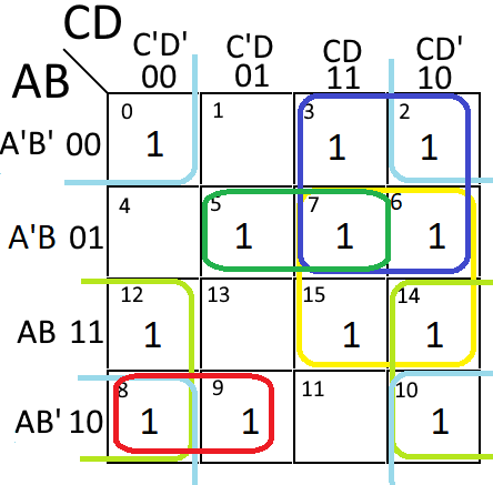
- \(a=A\overline{B}\overline{C} + \overline{A}BD + A \overline{D} + \overline{A}C + BC + \overline{B}\ \overline{D}\)
- a = red + dark green + light green + dark blue + yellow + light blue
- Now we can make a logic circuit out of the expression
- Repeat the process for the remaining segments and then you can combine the circuits to complete the decoder
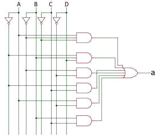
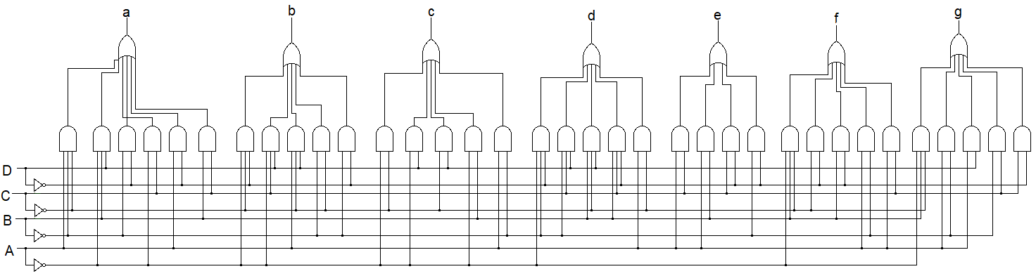
Explanation source: electronics-fun.com
- This process is an example of combinational logic circuits, which unlike sequential logic circuits (i.e. flip-flops), these do not have states, so they are much simpler and we could replace them with a lookup table in the form of an EEPROM
- The ABCD variables act as the address bits and the a, b, c, d, e, f, g outcomes are the data contents that we program into the EEPROM such that it returns the decoded value that we want
- In runtime this memory is “read only” as it is intended just for lookups, and it saves us the hurdle of creating complex decoders
EEPROM
- ROM stands for read only memory
- It’s contents are manufactured and cannot be changed
- PROM stands for programmable read only memory
- Let’s you programm it once and read it multiple times
- EPROM stands for erasable programmable read only memory
- Let’s you program it multiple times by first erasing via ultra violet light
- EEPROM stands for electric erasable programmable read only memory
- Organized as arrays of floating-gate transistors
- the gates are completely surrounded by highly resistive material
- the charge contained in it remains unchanged for long periods of time, nowadays typically longer than 10 years
- You can re-program them electronically multiple times without needing to expose them to ultra violet light
- Organized as arrays of floating-gate transistors
- We’ll be using the AT28C16 EEPROM
- CMOS based but CMOS & TTL Compatible Inputs and Outputs
- 7 input/output (I/O) pins
- 11 address lines (to specify which address we want to program/read)
- \(\overline{WE}\) = active low write enable
- \(\overline{OE}\) = active low output enable
- \(\overline{CE}\) = active low chip enable
- When the EEPROM are erased/brand new, they are erased with all 1’s
- To program the contents of the EEPROM you set \(\overline{WE}\) or \(\overline{CE}\) low and \(\overline{OE}\) high and the I/O pins now behave as input pins
- We’re gonna go with \(\overline{WE}\)
- The datasheet specifies the timing of certaing pulses (when and for how long should paramaters values be inputted to the chip) to trigger a writting
- We need to keep the write pulse signal between 100 and 1000 nanoseconds
- When the write enables goes low, it will latch the addres for at least 50 ns (\(t_{AH}\))
- The address has to be set up to \(t_{AS}\) ns prior to that
- The inputted data will be latched when the write enables goes back high again for 10 ns (\(t_{DH}\)).
- the data should have been inputted prior to that for up to \(t_{DS}\) ns to that
- We don’t have to worry about setting the address/data in advance since there is no limit for how much time in advance we set up those pins.
- The only timings we should be aware of are the write pulse and the write cycle time, for which we will use the RC circuit to generate a pulse
- Since we are inputting the changes manually, we can actually ignore the write cycle time as there’s no human way to insert new data and press the pushbutton before \(t_{WC}\) max time.
- Remember that as we observed in the D flip-flop, with the voltages that we’re using \(RC\) was a good estimation for high/low logic swaps.
- We shouldn’t worry about \(\overline{WE}\) double clock pulses either because the reason it happened was from the capacitor discharging in the direction from where it got charged, that affected other modules connected to the clock signal before. However, in this scenario there is no other module connected to the same signal feeding the capacitor, and the only component connected to the capacitor is on the side that won’t receive the discharging signal.
- We have to achieve an RC circuit with T between 100 and 1000 ns
- A capacitor in the nano farad get’s us in the nano seconds range, together a resistor between 100 and 1k Ohm should do the trick.
- Check this useful table for capacitor values
- This “edge” detector circuit has to actually be negative. Stable high and then a sharp decrease to low that bounces back to high. It can be achieved in 2 ways:
Positive RC edge detector circuit
- Using a smiliar RC logic we used for the RAM (and we can borrow ahead from the kit either a NAND gate or a hex inverter to invert the signal like for the RAM), see the circuit below with the left 1 Mega ohm resistor * 100nF (104 capacitor) = 0.1s pulse resistor circuit:
- The circuit is stable low because the capacitor gets charged quickly via the RC resistor (A) (and becomes open circuit) and the input draws (or rather, sinks) the current from the pull-down resistor on the right (B).
- When the button is pressed the capacitor decharges fast to ground via the pushbutton (the input remains low)
- Upon release the capacitor starts to get charged again via the RC resistor (A) connected to VCC, while it’s charging (up to a thertain threshold) the input briefly becomes high. The charge time is the pulse time, until the capacitor becomes open circuit again and the input is stable low.
- It’s very hard to test long pulses with a LED since as the RC resistor increases (to check for a pulse visible to the human eye) the brightness decreases, you can see the tinkercad simulation below (which is slower than in real life) and the oscilloscope results:
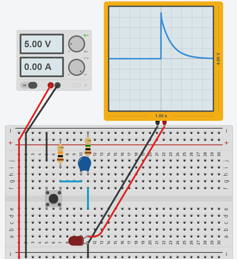 Open tinkercad
 - Note that we still need to invert the output (i.e. with a NAND, NOR or inverter chip)
- Note that generally the pull-down resistor has a much higher value than the RC resistor (the pull-down resistor has high resistance to keep power consumption low, the RC resistor has low resistance to keep the pulse short)
Negative RC edge detector circuit
- Alternatively, instead of using an inverter gate, we could just turn the pull-down resistor into a pull-up resistor (then this one becomes the RC resistor for the charge time)
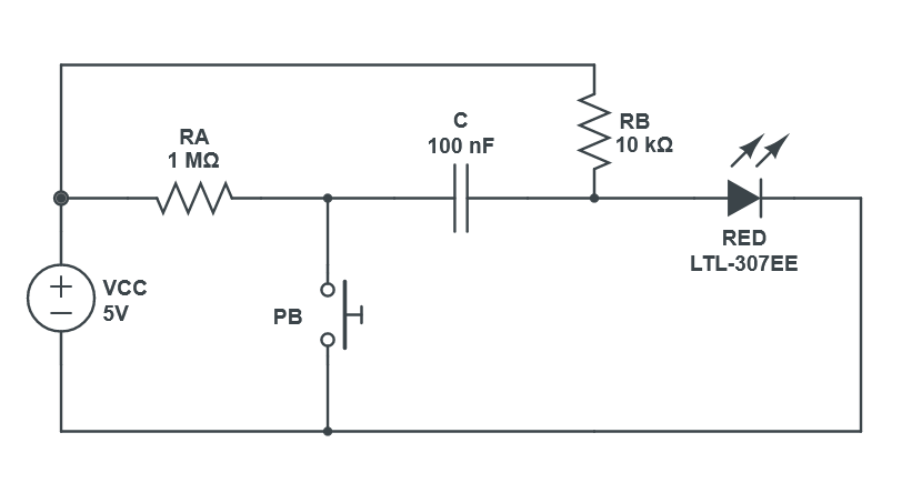
- The circuit is stable high as the capacitor charges via resistor A, immedieately becomes an open circuit, and resistor B feeds the input with high logic value.
- When the pushbutton is pressed, the capacitor will quickly decharge to ground, and subsequently for that time the circuit has low input. While still pressing, the capacitor eventually gets charged by resistor B, and when that happens the capacitor becomes an open circuit and the pull-up resistor feeds the input again. (high) That time is the negative pulse time, therefore resistor B is the RC resistor.
- After release, the capacitor decharges via the input (keeps it high)
- You don’t want to have RA as a pull-down resistor because then the current comming from resistor B will very unlikely diverge any to the capacitor, making the whole pushbutton useless and the state always high.
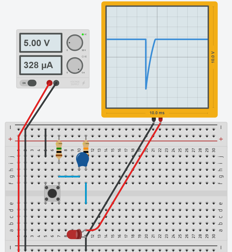 Open tinkercad
- Using a smiliar RC logic we used for the RAM (and we can borrow ahead from the kit either a NAND gate or a hex inverter to invert the signal like for the RAM), see the circuit below with the left 1 Mega ohm resistor * 100nF (104 capacitor) = 0.1s pulse resistor circuit:
- We’re gonna go with \(\overline{WE}\)
Breadboard circuit to program/debug the EEPROM
With a breaboard and jumperwires:
- Set up power/ground pins
- Set \(\overline{CE}\) to ground
- Hook up LEDs to the I/O pins with resistors in series
- I/O0 = least signicant output LED
- Use an 8-bit DIP switch with one terminal connected to the EEPROM addresses and to ground with 10k ohm resistors and the other terminal connect it to \(V{cc}\)
- LSB of 8-bit switch = A0 (pin 8)
- Use a 4-bit DIP switch to do the same with the remaining 3 addresses, note that the \(V_{cc}\) and pull-down resistors are swapped to other side and the top switch should be left unused.
- MSB of 4-bit siwtch = A10 (pin 19)
- Set the address and data contents beforehand (i.e. with jumperwires to \(V_{cc}\) or ground)
- Make an RC circuit with 2 pull-up, resistors a capacitor, and a pushbutton
- In practice, it may still work if we exceed the time specified by the datasheet, so we might just try to use or smallest resistor and capacitor values available in the kit.
- Connect the left leg of the pushbutton to ground
- Connect the right leg of the pushbutton to pull-up resistor A
- Connect the capacitor with one leg connected to pull-up resistor A and the other leg connected to RC (pull-up) resistor B and the \(\overline{WE}\) pin.
- pull-up resistor A value: standard pull-up value such as 10k
- (pull-up) RC resistor B value: anything between 100 and 1000 ohm if you use a 1nF capacitor, such as 680 ohm. Only 220 is included in the kit (can put 2-4 in series)
- capacitor value: 1nF (102 capacitor code), not included in the kit. Often this capacitor has a variable value depending on the temperature, the 0.1nF (101) capacitor is more stable and could be combined with a 2k-8k resistors.
- Then you can store data by setting the address with the DIP switches and the contents with the I/O jumperwires before pressing the pushbutton, then press the pushbutton to save.
- You need to have \(\overline{OE}\) high, otherwise it would not let you save (it’ll just output the contents of the EEPROM at the selected address)
Tinkercad
- Alternatively, check how to build an Arduino EEPROM programmer
8-bit decimal display
- We’ll use the EEPROM as a binary to decimal decoder for 1 byte to 3 decimal digits and a minus sign (4 LED displays)
- EEPROM “look up table”: we’ll use the outputs of a decoded binary counter and a 2’s C signal as the MSB bits of the EEPROM address, which has another 8 bits of inputs (namely an 8 bit binary number) for which we can program the following outputs:
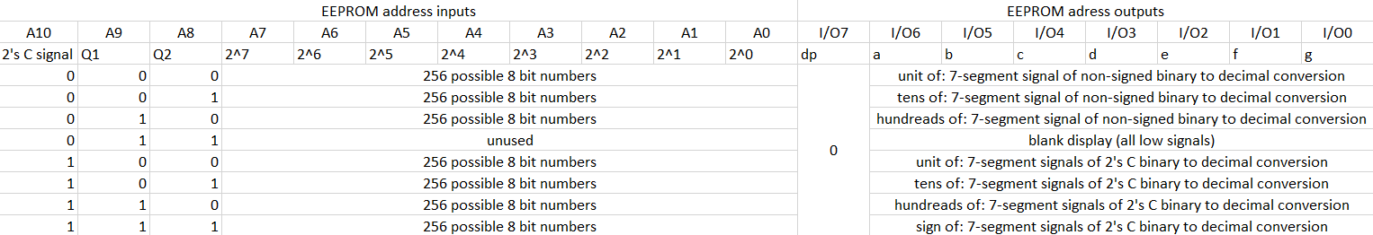
- Example for 123:
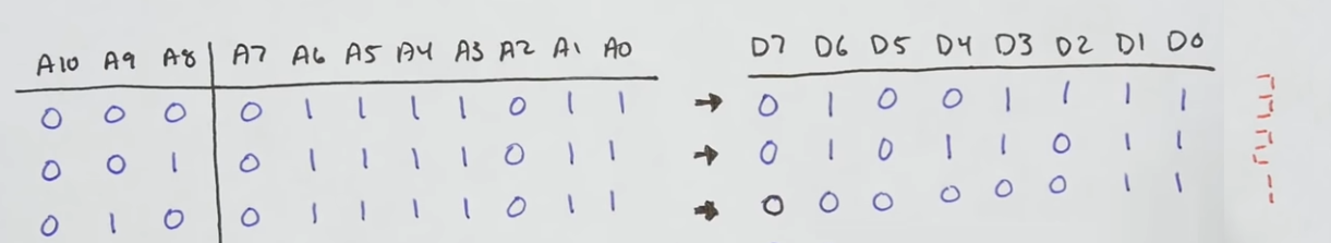
- EEPROM “look up table”: we’ll use the outputs of a decoded binary counter and a 2’s C signal as the MSB bits of the EEPROM address, which has another 8 bits of inputs (namely an 8 bit binary number) for which we can program the following outputs:
- All 4 LED displays will get virtually the same address signal (i.e. the binary number stored at the output register), but only the 8 LSB address bits are the same.
- The remaining 3 MSB address bits will be used to decode the unit’s place, the tenth’s place, the hundreadth’s place and the negative sign.
- We will tie each common cathode/anode of the LED to a uniquely decoded pin out of a 2-bit binary counter made from JK flip-flops, each LED is on average “on” only a fourth of the time.
- The cycle (clock) speed will be so fast, that the human eye wont be able to see that the numbers are being powered on and off, it’ll look as if both 4 LED displays are on at the same time.
- Evenutally what we are doing is cyclying through displaying only the units, only the tenths, only the hundreads, only the negative sign.
Steps:
- Program the EEPROM and conect its pins
- An example can be found in this forked repository
- Chip enable to ground
- Output enable to ground
- Write enable high
- A0-7 as jumperwire signals until building output register
- Insert 3 LEDs and its common cathode to ground with a 1k resistor.
- Connect the 8 EEPROM I/O pins (although here they will just be regarded as outputs) to the first 7 segment display as given in Ben’s schematic
- A goes to 7th bit (I/O 6)
- B goes to 6th bit (I/O 5)
- …
- G goes to D0
- DP (decimal point) goes to 8th bit I/O 7
- I might have damaged D7 of the EEPROM and always have a high value for D7 and we don’t use decimals anyway so I’ll tie them both to ground.
- Update: it was a bug in the code that always skept the msb, just had to fix the “foor loop” boundaries.
- Connect all 7-display segments A’s with A’s, B’s with B’s… such that all 3 LEDs are getting the same EEPROM signals
- Build a astable 555 timer clock that we will use to cycle through the LED displays
- Connect ground and power
- Connect \(2\mu F\) capacitor from pin 2 to ground
- Connect pin 2 to pin 6
- Connect pin 5 to ground with a 10nF capacitor (103)
- Put a 100k resistor between pin 6 and 7
- Put a 1k resistor between pin 7 and \(V_{cc}\) (or 8, which also is VCC)
- Build a binary counter out of the 74LS107 Dual (master-slave based, so no racing problem) JK flip flops
- 74LS107 toggles at high clock pulse
- Set power and ground pins
- Set clear high (for both flip flops)
- Set J and K high (for both flip flops)
- Connect the output of the 555 timer into the the CLK of the first flip flop
- Connect the output of the first flip flop into the CLK of the 2nd flip flop
- Connect the outputs of the binary counter we just built to the the address pins of the EEPROM:
- A8 = Q2
- A9 = Q1
- A10 = 2’s Complement signal
- Use Q2 and Q1 also to control which LED display to light up by making them inputs of the 74LS139 decoder and connecting the cathodes to each decoded output:
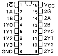
- Connect power/ground pins
- Connect counter Q1 to A, counter Q2 to B
- Connect Y0 with units LED cathode, Y1 with tens, Y2 with hundreads, Y3 with minus sign
| Q2 (B) | Q1 (A) | Y3 | Y2 | Y1 | Y0 | active LED |
|---|---|---|---|---|---|---|
| 0 | 0 | H | H | H | L | units |
| 0 | 1 | H | H | L | H | tens |
| 1 | 0 | H | L | H | H | hundreads |
| 1 | 1 | L | H | H | H | minus sign |
- Result: we’re both, displaying the correct LED, and inputting the correct EEPROM address at the same time
- After debugging, you should speed up the clock speed by changing the rc values. Replace the \(2\mu F\) with a 10nf (103)
“Tinkercad”
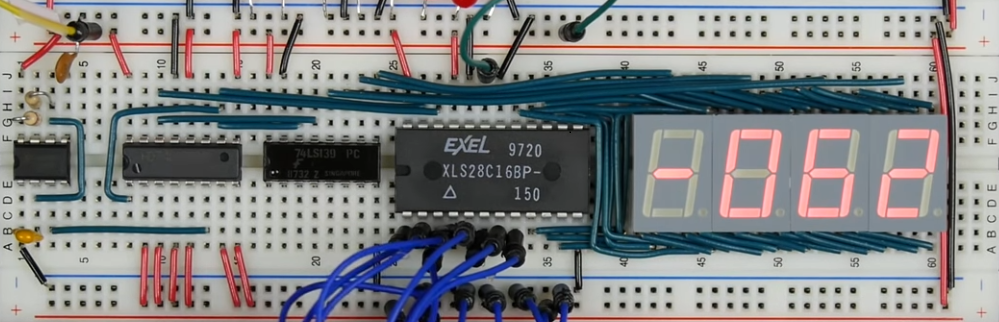
- Ben is using a 74LS76 as the dual JK flip-flop but the kit comes with the 74LS107, which is functionally the same, but has a different pinout:
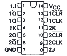 (74LS107 pinout)
 - We can cover the output LEDs with a transparent red plastic to improve its readability
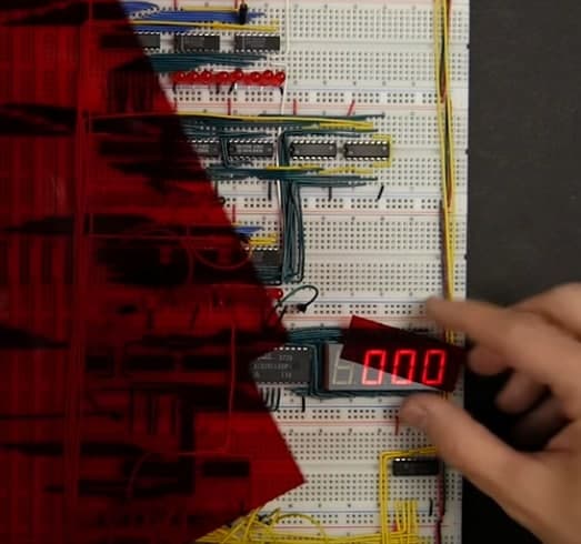
Output register
- It doesn’t need to drive the Bus, it only needs to read from the Bus, therefore the tri-state buffer gate wont be needed
- Instead of using two 74LS173 (4-bit registers) we’re gonna use the 74LS273, which is an 8 bit register.
- The ‘173 has an input enable AND a clock pin, whereas the ‘273 only has a clock pin.
- This means that every time the clock pulses, the ‘273 will latch in whatever is on the bus, no matter what.
- We solve this by AND’ing the clock signal with the input enable signal.
- Potential problem: you may get random voltage spikes on your control lines
- Potential solution: Replace the ‘273 with two ‘173s (like the other registers) and (completely doing away with the AND gate). You could also use an 8-bit register chip that has an input enable.
- 74LS273 pinout:
- Connect power/ground pins
- Connect outputs of the register to EEPROM address inputs A0-A7
- Use a jumperwire signal for MR (master reset), connect it high
- insert an and gate (74LS08) and its power/ground pins
- Connect AND gate output to register CLK
- Hookup a control signal jumperwire to one of the AND inputs
- The other input is the system clock signal
- Connect all output register inputs to the bus
Schematic
Output module
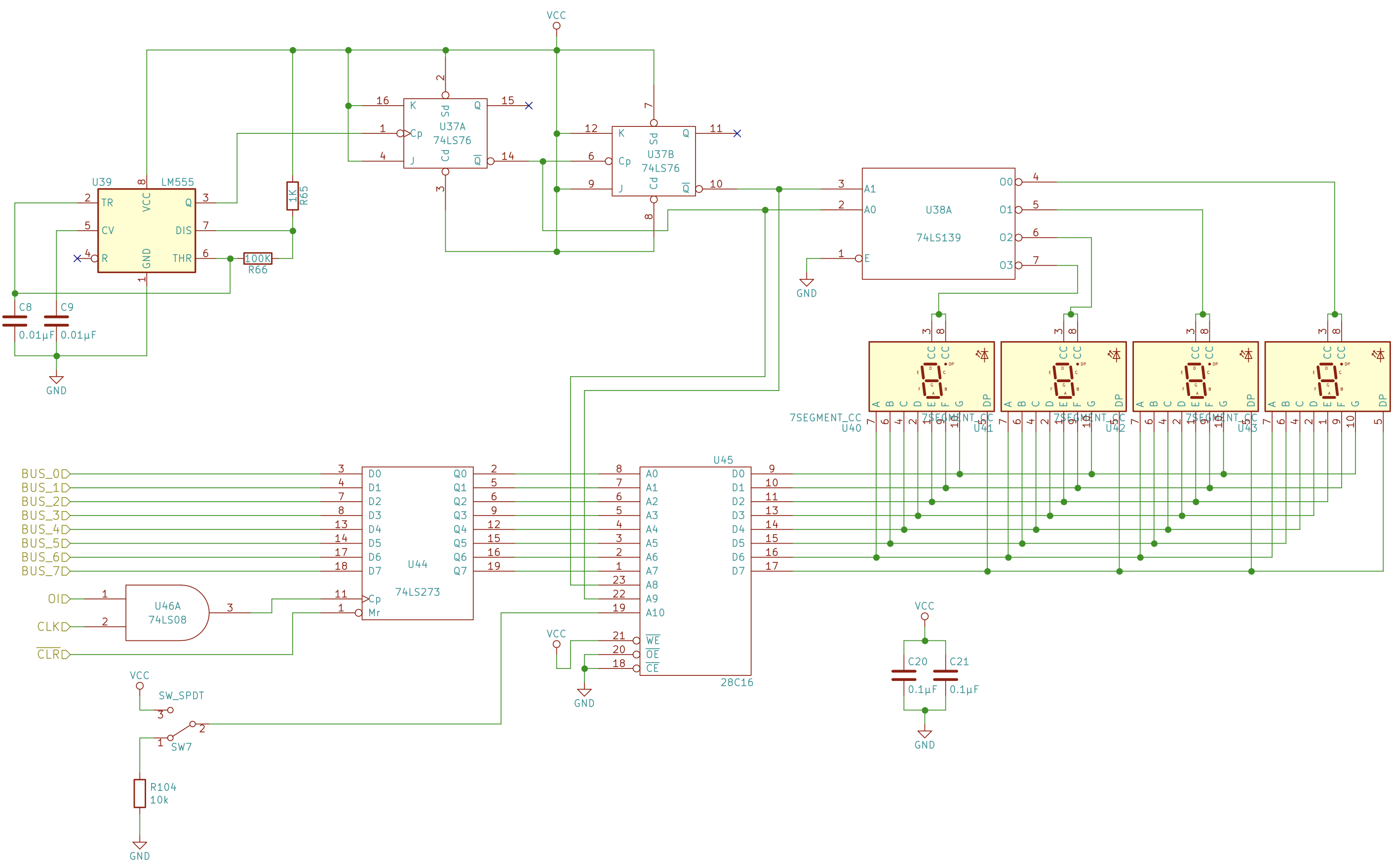
Computer High Level overview so far
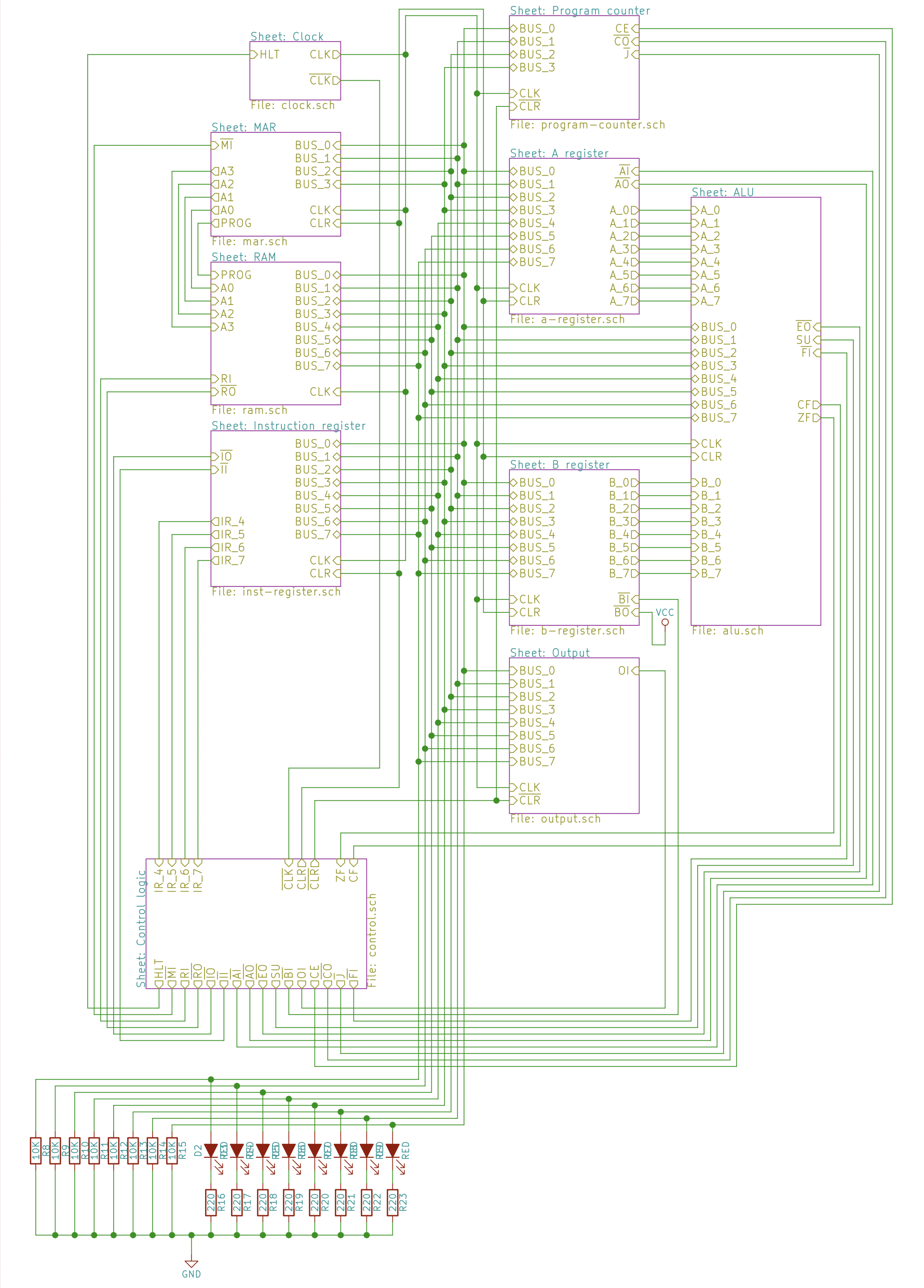
Terminology review
Instruction set architecture
- “An instruction set architecture (ISA) is an abstract model of a computer that serves as the interface between software and hardware”
- Basically it’s a set of definitions and graphs that help the user understand the hardware behind the software features provided
- The ISA provides:
- supported data types (in our case only 8 bit integers)
- memory layout
- addressing modes (we have 16 “byte addressable” addresses)
- instruction set (implicit meaning of all the bits that we program at each byte of the RAM)
- This is arbitrary and we will create our own instruction set language (which we will refer to as machine language)
- While “binary instruction/opcode” refers to the meaning that we free willingly assign to a binary string, an assembly language opcode is the human readable version of it.
- “Instruction set/machine language” then refers to all the meanings that we give to our programmable bits.
- Our instruction set is of fixed length, namely one instruction takes one RAM address of space, this makes it very simple to fetch for next instructions (just increment the address).
- input/output model (ours doesn’t have “interrupts” besides input halts, which are determined by the program)
- There are various types of ISA’s, such as CISC (stack based) and RISC (register based). Ours is so limited we can’t really compare it to any commercial ISA, it’s our own ISA.
Memory layout of a stored-program digital computer
- Below a review of the von Neumann architecture that we’ll use to establish some terminology (especially CPU terminology) and see how our computer compares to this established framework of “stored-program digital computer”
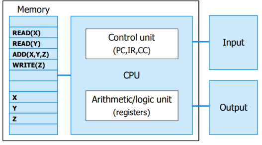
- the von Neumann architecture describes a design architecture for an electronic digital computer with these components:
- A processing unit (CPU) that contains an arithmetic logic unit and processor registers (A, B and flag registers)
- A control unit that contains an instruction register and program counter
- Memory that stores data and instructions
- External mass storage (we don’t have this)
- Input and output mechanisms
- Note that although a “live” input during run mode was not a feature of Ben’s build I’ve decided to do a poorman’s “live” input implementation just by adding one extra switch and an Input “protocol” based on the operand of the HLT command (see the footnote at the instruction set section).
- Although these are formal definitions beyond Ben’s project goal, it was a goal of mine to understand computer jargon, hence this slight theory detour.
Computer vs CPU vs Control unit
- Looking at the von Neumann architecture that we have, we can see at a higher level that the “CPU” (central processing unit) in a computer is composed of the ALU (the module that does all the calculations) and the Control Unit, which is responsible for fetching, decoding and executing instructions stored in the program.
- PC = program counter
- IR = instruction register
- CC = control circuitry (partially called “control word” by Ben)
- Taking von Neumann terminology into account, this is what the architecture and terminology of our 8 bit computer looks like:
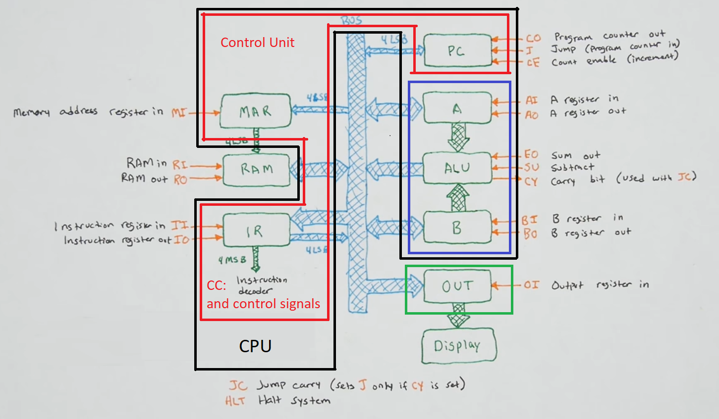
- “CPU” would consist of the red and blue bordered areas, with the read one being the control unit and the blue one the ALU.
- The RAM is the memory that contains the program and variables, but as described in the memory layout section, we could define address 1111 and a halt/unhalt mechanism to integrate “live” user inputs by explicitly storing them in the last RAM address.
- What it’s left to do is the control circuitry and integrating the components of the control unit:
- Brush up active low signals
- Invent a machine language/instruction set
- Implement instruction decoders and their integration with the program counter and instruction register.
Control unit
Cleaning up control circuitry
- Before we start integrating the control unit, we will first “fix” the active low signals into active high to keep things consistent which then make it easier to integrate and debug.
- Replace all jumperwires with long cables that we will connect to a “hub” of control signals, which are part of the “control circuitry” in CSE1400 or (“control word” by Ben) together with the instruction decoder (called EEPROM microcode by Ben) to which all these signals connect.
- We will also connect these signals to LED and resistors (that connects to ground) in series to be able to see their state (high or low) and eventually connect them (before the anode) to the output pins of the “Microcode EEPROMs”, which act basically as instruction register opcode decoders, and control whether a signal is high or low.
- With the active low signals, we will invert active lows with an HEX inverter chip to make “microcode” easier
- I burned one hex inverter so I decided to use un-used inputs of other NAND and hex inverter chips used in other modules
- Replacing the jumperwires with long wires should look like this:
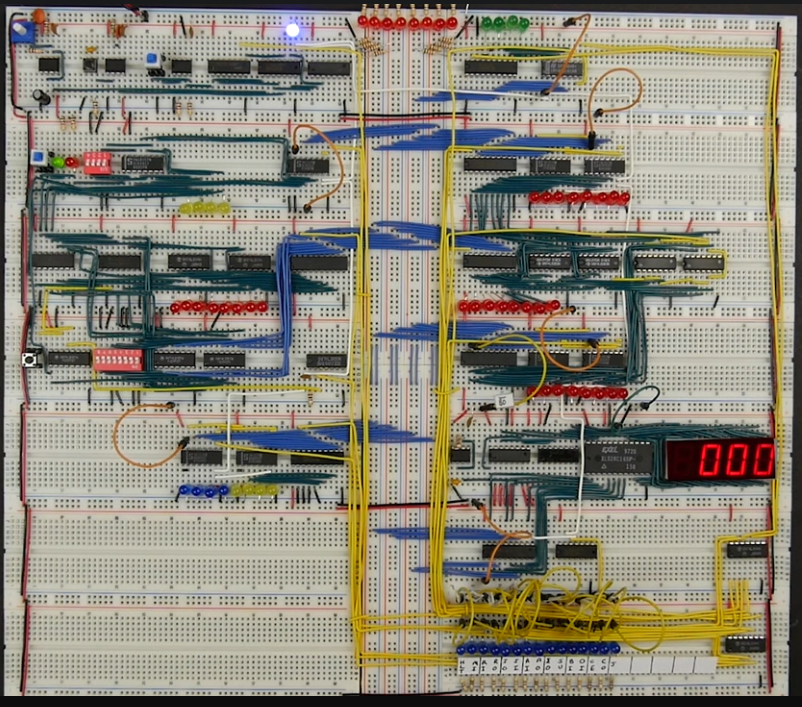
Defining our own assembly language
Example
- Recall that machine language/instruction set is the binary code that we will input in the RAM and that assembly language is the human readable version.
- Let’s come up with an example of a 3 word command pseudocode for our “machine language” and define how we would execute it:
  0. LDA 14
  1. ADD 15
  2. OUT
- All of our programs implicitly start at RAM address 0, and since our instruction length matches the byte addressable memory locations, each line of code number literally represents the RAM address in which we will store that “line of code” or rather instruction.
- This means that first we load the contents of memory address 14 into register A
- Then we load the contents at address 15 into register B
- Then we load the contents of the ALU into the output register
Instruction format
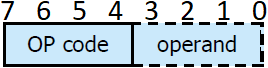
- All of our instructions would have the following layout in memory:
[4-bit instruction (known to humans as opcode)] (4-bit operand)with [] defining mandatory and () defining optional.- This already tells us that we have a maximum of 16 opcodes
- The optional operand may not be used (whatever is on the 4 LSB is ignored) because the address/register is implicitly known or because it does not regard any storage, such as halting the clock.
- This is known as one-address instructions, where the implicit register in commands such as
SUM OUTandSTORE 10is the so called “accumulator” (holds temporary results of the ALU), which in our case is not a seperate register but the actual contents of the two 4-bit adders that make up our ALU, and the operand generally stands for a register, constant or memory address. - Our operands will regard either a memory address or an immediate value (a 4 bit integer)
Instruction set
- The table below shows the complete list of 4-bit binary instructions and their human readable opcodes
| binary instruction | assembly opcode | has operand | meaning |
|---|---|---|---|
0000 |
NOP | no | Do nothing (no operation) |
0001 |
LDA | yes | Load contents of operand address into register A |
0010 |
ADD | yes | Load contents of operand address into register B, and set ALU to sum (default), then store result into register A |
0011 |
SUB | yes | Load contents of operand address into register B and set ALU to subtract, then store result into register A |
0100 |
STA | yes | Store the contents of register A into the address of the operand |
0101 |
LDI | yes | Load immediate value of the operand into register A |
0110 |
JMP | yes | Jump to the memory address of the operand (aka code line) |
0111 |
JPC | yes | Jump to the memory address of the operand if last operation had a 9th bit carry |
1000 |
JPZ | yes | Jump to the memory address of the operand if the last operation resulted in zero |
1110 |
OUT | no | Load contents of register A into output register |
1111 |
HLT | yes\(^{[1]}\) | Halt the system |
[1]: To implement a cheap “live input” feature we can establish that HLT with 0000 operand means the normal HLT that Ben implemented (Usually end of the program and everything has to be reseted/cleared). However, when there is a non-zero operand we can establish that HLT is prompting the user to store an input (thus switching back to program mode) in the memory address pointed by the operand, then the user has to switch back to run mode and hit the reset button with the “clear switch” off (this is my own modification to Ben’s build).
Control logic
- In order to execute an instruction such as
00011111(LDA 15), which stands for “Load contents of operand address into register A”, we have to to trigger certain signals high (the rest are implicitly low) to ensure we move the data that we want in the correct places without corrupting it. - Steps to run any instruction (
00011111as an example):- Fetch cycle: We fetch the instruction from memory and put it in the instruction register.
- Go to next instruction (pointed by the program counter): Program counter out -> Memory address register in
- Send opcode to instruction decoder: RAM out -> Instruction register in
- Increment program counter already for next instruction: Counter Enable
- Although it has a seperate logical purpose, we will include Counter Enable into the previous clock cycle as it does not interfere with the Bus, so we save up 1 micro clock cycle.
- Decode instruction: Here the instruction decoder will know that
00011111means take the contents of memory address1111and put it on register A - Execute instruction
00011111:- Instruction register out (this outputs the lower significant bits that contain the address of the operand) -> Memory address register in
- Ram out -> Register A in
- Fetch cycle: We fetch the instruction from memory and put it in the instruction register.
- In practice the decode will be done by using an EEPROM (we can replace combinatorial logic with a EEPROM) and the execution takes multiple clock cycles. In this case we saw that it took 2 clock cycles for the execution.
- In practice the execution is not necessarily a different process from decoding, they go hand in hand and as at each clock cycle the EEPROM will decode a different set of control signals that get executed within the same rising edge of the clock.
- Splitting one instruction/opcode into different clock cycles results in multiple “micro instructions” that take 1 clock pulse each.
Building the control logic counter
- we need to be able to know in which micro instruction number we are and start from 0 again when we’re done executing all the microinstructions
- We build a separate program counter but for micro instructions.
- This one is much simpler than the program counter as micro instructions do not have jumps
- Every micro instruction takes 1 clock cycle so there’s no need to have a counter enable signal (it’s always on)
- When we’re done we can just reset the clock to 0. (which immedeately starts the next fetch cycle)
- The values of this separate counter indicate the micro instruction number that is being executed, and we call those numbers T0, T1…
- we’re just gonna use the lower 3 bits out of the 4 that the 74LS161 4-bit binary counter has)
- As a matter of fact, we’re just gonna have a total of 5 micro instruction clock cycles and all microinstructions will have the same length (we just padd the remaining cycles with no operation at all). We will reset the micro clock after the 5th cycle, this is easier to implement than to have an extra control signal that resets the micro clock.
- Implementation:
- Insert the 74LS161 4-bit binary counter
- Connect power and ground
- Tie clear (for now) and load high, as well as 7 and 10 (enable)
- Connect the global computer clock signal to the clock pin after offsetting it
- Offset the control logic counter:
- We need some buffer time to prepare the control signals before the next clock cycle comes in. If we just use the same clock pulse as the global computer, the control signals may or may not be updated for the clock pulses that we need.
- By using an inverted global clock signal for the micro instructions clock we then can prepare the control signals while the global clock is low (as ours will be high). Eventually the micro instruction clock gets incremented at the falling edge of the global clock.
- We already inverted the global clock twice for the RAM RC circuit. Just use the first inversion also for the micro instruction clock.
- Use the 74LS138, which is a 3-8 line decoder, because we want to convert the 3 bit input of the micro clock into 8 separate signals, of which we will use just 6 (5 to light up LEDs that help us debug), and the 6th bit (bit Q5 if we start counting at Q0) will be used to reset the micro clock (since T5, T6 and T7 will never be used) (recall that the decoder has all H except 1 L)
- so basically we have 5 T’s for each opcode for which we can program a microcode instruction (a set of high and low control signals)!
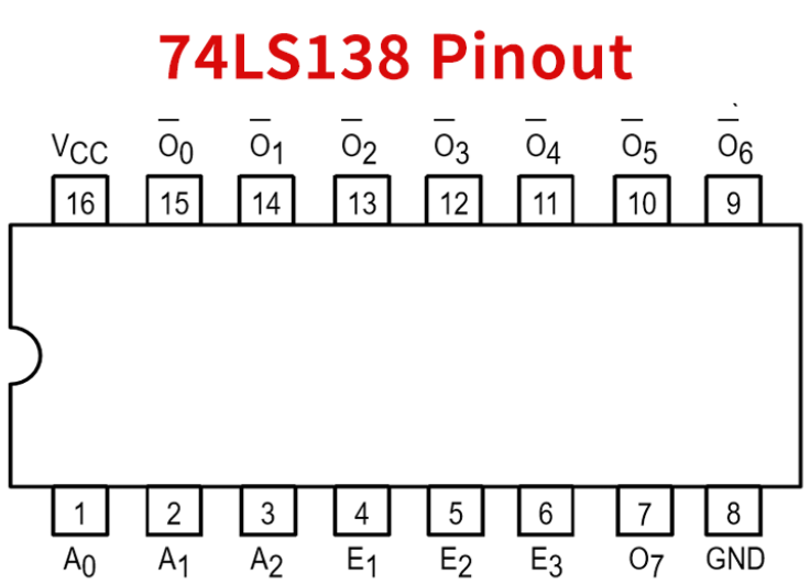
- Hookup ground and power
- \(E_1\) and \(E_2\) are active low while \(E_3\) is active high, connect the first 2 to ground and the third one to \(V_{cc}\)
- Hookup the inputs to the micro code clock outputs (both chips are big endian (LSB pins start on the left))
- Connect clear of the micro clock to the 6th output bit (Q5) of the decoder
- so basically we have 5 T’s for each opcode for which we can program a microcode instruction (a set of high and low control signals)!
- Insert the 74LS161 4-bit binary counter
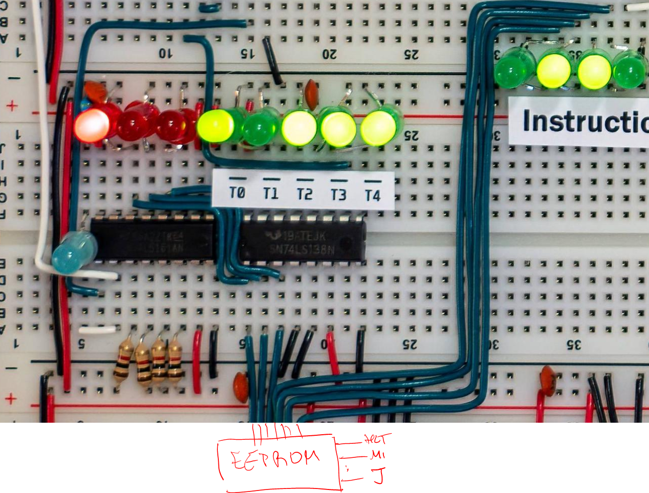
Building the flags register
- To make the computer turing complete we need a conditional signal that triggers an instruction based on a previous state state of the CPU (i.e. the last ALU operation was equal to zero) such as “JZ” (jump zero), which jumps only if the last operation was zero.
- If the conditional signal didn’t meet the requirements, then the instruction decoder shall just move onto the next line of code just like if the instruction was a NOP.
- To be turing complete just 1 conditional condition is enough.
- The flags register is the status register that contains the state of the CPU, such as
boolean“last operation outcome is zero” andboolean“last operation had 9th bit carry”, which are the ones that we’re gonna implement.- Jump carry can happen in multiple ways:
- The addition of two positive bytes is greater than 255 and thus there is carry bit overflow
- Subtracting A with any originally positive 8-bit number will yield 9th carry unless A is 0.
- So by preceeding A - 1 JC will be like jump if A != 0
- To enable the flags register to update the booleans we add to the last micro step of ADD and SUB instructions the “FI” (flags in) signal, which is the enable signal of the 4-bit register we will use for the flags.
- Jump carry can happen in multiple ways:
- JC implementation:
- Chain the carry out of the most significant 4-bit adder of the ALU to the a data pin of the flags register
- JZ implementation
- Use NOR gates which are feed with the ALU output, which should be equal to 1 only if all inputs are 0.
- the 74LS02 NOR gate has for 2-input NOR gates, we can feed 4 pairs of the 8-bit ALU output into the chip and then AND them together with the 74LS08
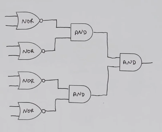
- Steps:
- Insert the 74LS02 and 74LS08 next to each other
- Hookup power/ground pins
- Hookup the outputs of the 2 NOR gates in the bottom to the inputs of the first AND gate in the bottom
- Hookup the outputs of the 2 NOR gates in the top to the inputs of the first AND gate in the top
- Connect the outputs of the 2 AND gates to the output of the third AND gate (also on the top)
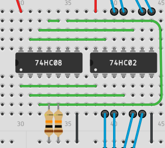 Open tinkercad
 - Connect the ALU outputs to the inputs of the NOR gates (doesnt matter the order)
- Insert the 74LS173 chip and connect power/ground pins
- Connect the carry and the zero flags to an input pin each (MSB) of the flags register. Connect 10k pull-ups to the other input pins.
- We want the output of the 173 to always be enable, so connect both M and N (pins 1 and 2) to ground (active low)
- Connect the 2 MSB outputs to blue LEDs with resistors in series
- 10b connect the Carry flag output to address pin A8 and Zero flag output to address pin A9 of the microcode EEPROMs
- Connect the clock pin to the system clock
- Merge pin 9 and 10 (enable) and connect it to the output pin of the nearest hex inverter/NAND gate output available.
- 12.b: Connect the FI control signal to the inputs of that inverter gate
- Connect the clear pin to the nearest/most accesible clear pin of another register
Schematic
Building the fetch cycle
- The first 2 microinstructions that constitute the fetch cycle are the same for all opcodes.
- Altough we don’t need to know the instruction register opcode, it’s easier to implement the fetch cycle microinstructions decoder together with the instruction decoder EEPROMs.
Building the instruction decoder
- In order to decode a whole instruction (including the fetch cycle) we will append the micro clock cycle outputs together with the opcode, the carry and the zero output pins of the flags register and the Left (gnd)/Right(vcc) setting and connect them to the address pins of the EEPROMs, which should return, for each T, a set of high/low control signals, which may vary depending on the conditional flags.
- The lookup table below summarizes what we expect the EEPROM to output for each control signal based on the instruction opcode (and micro-clock step value)
- The Left/Right EEPROM address pin is just to divide the 16 bit control word into the 8 MSB outputs and the 8 LSB outputs, but the lookup table skips this and just shows the full 16 bit control word regardless of the Left/Right EEPROM setting.
- Note that for most instructions the lookup table output will be the same regardless of the flags input and only for the conditional jumps the flags inputs will matter.
- Repo with the EEPROM code to program (store) the table below with arduino
| Assembly opcode | CF | ZF | Binary opcode | Microclock Step | HLT | MI | RI | RO | IO | II | AI | AO | EO | SU | BI | OI | CE | CO | J | FI |
|---|---|---|---|---|---|---|---|---|---|---|---|---|---|---|---|---|---|---|---|---|
| (Fetch) | x | x | xxxx | 000 | 0 | 1 | 0 | 0 | 0 | 0 | 0 | 0 | 0 | 0 | 0 | 0 | 0 | 1 | 0 | 0 |
| x | x | xxxx | 001 | 0 | 0 | 0 | 1 | 0 | 1 | 0 | 0 | 0 | 0 | 0 | 0 | 1 | 0 | 0 | 0 | |
| LDA | x | x | 0001 | 010 | 0 | 1 | 0 | 0 | 1 | 0 | 0 | 0 | 0 | 0 | 0 | 0 | 0 | 0 | 0 | 0 |
| x | x | 0001 | 011 | 0 | 0 | 0 | 1 | 0 | 0 | 1 | 0 | 0 | 0 | 0 | 0 | 0 | 0 | 0 | 0 | |
| x | x | 0001 | 100 | 0 | 0 | 0 | 0 | 0 | 0 | 0 | 0 | 0 | 0 | 0 | 0 | 0 | 0 | 0 | 0 | |
| ADD | x | x | 0010 | 010 | 0 | 1 | 0 | 0 | 1 | 0 | 0 | 0 | 0 | 0 | 0 | 0 | 0 | 0 | 0 | 0 |
| x | x | 0010 | 011 | 0 | 0 | 0 | 1 | 0 | 0 | 0 | 0 | 0 | 0 | 1 | 0 | 0 | 0 | 0 | 0 | |
| x | x | 0010 | 100 | 0 | 0 | 0 | 0 | 0 | 0 | 1 | 0 | 1 | 0 | 0 | 0 | 0 | 0 | 0 | 1 | |
| SUB | x | x | 0011 | 010 | 0 | 1 | 0 | 0 | 1 | 0 | 0 | 0 | 0 | 0 | 0 | 0 | 0 | 0 | 0 | 0 |
| x | x | 0011 | 011 | 0 | 0 | 0 | 1 | 0 | 0 | 0 | 0 | 0 | 0 | 1 | 0 | 0 | 0 | 0 | 0 | |
| x | x | 0011 | 100 | 0 | 0 | 0 | 0 | 0 | 0 | 1 | 0 | 1 | 0 | 0 | 0 | 0 | 0 | 0 | 1 | |
| STA | x | x | 0100 | 010 | 0 | 1 | 0 | 0 | 1 | 0 | 0 | 0 | 0 | 0 | 0 | 0 | 0 | 0 | 0 | 0 |
| x | x | 0100 | 011 | 0 | 0 | 1 | 0 | 0 | 0 | 0 | 1 | 0 | 0 | 0 | 0 | 0 | 0 | 0 | 0 | |
| x | x | 0100 | 100 | 0 | 0 | 0 | 0 | 0 | 0 | 0 | 0 | 0 | 0 | 0 | 0 | 0 | 0 | 0 | 0 | |
| LDI | x | x | 0101 | 010 | 0 | 0 | 0 | 0 | 1 | 0 | 1 | 0 | 0 | 0 | 0 | 0 | 0 | 0 | 0 | 0 |
| x | x | 0101 | 011 | 0 | 0 | 0 | 0 | 0 | 0 | 0 | 0 | 0 | 0 | 0 | 0 | 0 | 0 | 0 | 0 | |
| x | x | 0101 | 100 | 0 | 0 | 0 | 0 | 0 | 0 | 0 | 0 | 0 | 0 | 0 | 0 | 0 | 0 | 0 | 0 | |
| JMP | x | x | 0110 | 010 | 0 | 0 | 0 | 0 | 1 | 0 | 0 | 0 | 0 | 0 | 0 | 0 | 0 | 0 | 1 | 0 |
| x | x | 0110 | 011 | 0 | 0 | 0 | 0 | 0 | 0 | 0 | 0 | 0 | 0 | 0 | 0 | 0 | 0 | 0 | 0 | |
| x | x | 0110 | 100 | 0 | 0 | 0 | 0 | 0 | 0 | 0 | 0 | 0 | 0 | 0 | 0 | 0 | 0 | 0 | 0 | |
| JC | 0 | x | 0111 | 010 | 0 | 0 | 0 | 0 | 0 | 0 | 0 | 0 | 0 | 0 | 0 | 0 | 0 | 0 | 0 | 0 |
| 1 | x | 0111 | 010 | 0 | 0 | 0 | 0 | 1 | 0 | 0 | 0 | 0 | 0 | 0 | 0 | 0 | 0 | 1 | 0 | |
| x | x | 0111 | 011 | 0 | 0 | 0 | 0 | 0 | 0 | 0 | 0 | 0 | 0 | 0 | 0 | 0 | 0 | 0 | 0 | |
| x | x | 0111 | 100 | 0 | 0 | 0 | 0 | 0 | 0 | 0 | 0 | 0 | 0 | 0 | 0 | 0 | 0 | 0 | 0 | |
| JZ | x | 0 | 1000 | 010 | 0 | 0 | 0 | 0 | 0 | 0 | 0 | 0 | 0 | 0 | 0 | 0 | 0 | 0 | 0 | 0 |
| x | 1 | 1000 | 010 | 0 | 0 | 0 | 0 | 1 | 0 | 0 | 0 | 0 | 0 | 0 | 0 | 0 | 0 | 1 | 0 | |
| x | x | 1000 | 011 | 0 | 0 | 0 | 0 | 0 | 0 | 0 | 0 | 0 | 0 | 0 | 0 | 0 | 0 | 0 | 0 | |
| x | x | 1000 | 100 | 0 | 0 | 0 | 0 | 0 | 0 | 0 | 0 | 0 | 0 | 0 | 0 | 0 | 0 | 0 | 0 | |
| OUT | x | x | 1110 | 010 | 0 | 0 | 0 | 0 | 0 | 0 | 0 | 1 | 0 | 0 | 0 | 1 | 0 | 0 | 0 | 0 |
| x | x | 1110 | 011 | 0 | 0 | 0 | 0 | 0 | 0 | 0 | 0 | 0 | 0 | 0 | 0 | 0 | 0 | 0 | 0 | |
| x | x | 1110 | 100 | 0 | 0 | 0 | 0 | 0 | 0 | 0 | 0 | 0 | 0 | 0 | 0 | 0 | 0 | 0 | 0 | |
| HLT | x | x | 1111 | 010 | 1 | 0 | 0 | 0 | 0 | 0 | 0 | 0 | 0 | 0 | 0 | 0 | 0 | 0 | 0 | 0 |
| x | x | 1111 | 011 | 0 | 0 | 0 | 0 | 0 | 0 | 0 | 0 | 0 | 0 | 0 | 0 | 0 | 0 | 0 | 0 | |
| x | x | 1111 | 100 | 0 | 0 | 0 | 0 | 0 | 0 | 0 | 0 | 0 | 0 | 0 | 0 | 0 | 0 | 0 | 0 |
- Each of the outputs (row with 16 bits of high/low values for the control signals) are called control words.
- Since a control word is 16 bit long, we will need one EEPROM to output the 8 MSB signals and another EEPROM to output the 8 LSB signals.
- Breadboard circuit steps for the EEPROM instruction decoders:
- Get rid of the control signal jumperwires in the control hub
- Insert the EEPROMs and power/ground pins
- Set write enable high, output enable and chip enable low
- A10 won’t be used (we only have 3 bit micro clock + 4 bit opcode + A7 to determine 8 MS signals/8LS signals and A8 and A9 for the flags registers), so tie it to ground
- Tie the first EEPROM A7 to ground, the second one to \(V_{cc}\)
- Connect the remaining address pins in the following way
- A0 = Micro clock Q0
- A1 = Micro clock Q1
- A2 = Micro clock Q2
- A3 = IR Q4
- A4 = IR Q5
- A5 = IR Q6
- A6 = IR Q7
- Connect the I/O pins to the control signals in the following way:
- LEFT EEPROM:
- I/O0 = AO
- I/O1 = AI
- I/O2 = II
- I/O3 = IO
- I/O4 = RO
- I/O5 = RI
- I/O6 = MI
- I/O7 = HLT
- RIGHT EEPROM:
- I/O0 = FI (it’ll come later, skip for now)
- I/O1 = J
- I/O2 = CO
- I/O3 = CE
- I/O4 = OI
- I/O5 = BI
- I/O6 = SU
- I/O7 = EO
- LEFT EEPROM:
Building the reset circuit (resume clock and clear data)
- Because we also add a fetch cycle in the HLT opcode, an easy way to resume the program is to reset the microclock.
- The program counter has already been increased to the memory address next after the HLT codeline
- Ressetting the microclock puts T at 000 and the microinstruction is counter out & memory address register in, followed by T 001 (which has ram out, instruction register in and clock enable) which means that we successfuly moved past the HLT instruction.
| Assembly opcode | Binary opcode | Microclock Step | HLT | MI | RI | RO | IO | II | AI | AO | EO | SU | BI | OI | CE | CO | J |
|---|---|---|---|---|---|---|---|---|---|---|---|---|---|---|---|---|---|
| (Fetch) | xxxx | 000 | 0 | 1 | 0 | 0 | 0 | 0 | 0 | 0 | 0 | 0 | 0 | 0 | 0 | 1 | 0 |
| xxxx | 001 | 0 | 0 | 0 | 1 | 0 | 1 | 0 | 0 | 0 | 0 | 0 | 0 | 1 | 0 | 0 | |
| HLT | 1111 | 010 | 1 | 0 | 0 | 0 | 0 | 0 | 0 | 0 | 0 | 0 | 0 | 0 | 0 | 0 | 0 |
| 1111 | 011 | 0 | 0 | 0 | 0 | 0 | 0 | 0 | 0 | 0 | 0 | 0 | 0 | 0 | 0 | 0 | |
| 1111 | 100 | 0 | 0 | 0 | 0 | 0 | 0 | 0 | 0 | 0 | 0 | 0 | 0 | 0 | 0 | 0 |
- In addition to reseting the microclock, ben uses the same pushbutton to also reset the contents of all registers.
-
I want to be able to let the user prevent the reset from clearing all values and to clear only the clock such that we can just use the unhalt feature together with a new opcode that “prompts” the user for input and halts the computer. Naturally we wouldn’t want to clear everything afterwards…
- NAND gate based circuit and truth table for resetting both register data and micro clock
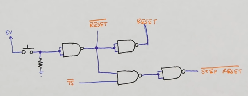
| Push button Reset | \(\overline{T5}\) | Active high resets | Active low resets | Micro clock reset |
|---|---|---|---|---|
| Inactive | 0 | 0 | 1 | 0 |
| Inactive | 1 | 0 | 1 | 1 |
| Pressed | 0 | 1 | 0 | 0 |
| Pressed | 1 | 1 | 0 | 0 |
- The reason Ben uses a buffer (triangle) is because it will now act as a buffer, or voltage follower. The idea is that if you took the signal from before a buffer, it could draw current and potentially burn out a chip, but a buffered signal will draw very little current.
-
The reason we invert one of the resets is because some resets are active high while others are active low
- With just a three terminal switch we can use it as a variable to determine whether the reset button clears the registers or not
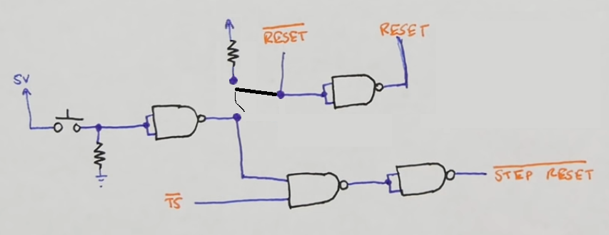
| switch common | Push button Reset | \(\overline{T5}\) | Active high resets | Active low resets | Micro clock reset |
|---|---|---|---|---|---|
| to pullup | Inactive | 0 | 0 | 1 | 0 |
| to pullup | Inactive | 1 | 0 | 1 | 1 |
| to pullup | Pressed | 0 | 0 | 1 | 0 |
| to pullup | Pressed | 1 | 0 | 1 | 0 |
| to \(\overline{button}\) | Inactive | 0 | 0 | 1 | 0 |
| to \(\overline{button}\) | Inactive | 1 | 0 | 1 | 1 |
| to \(\overline{button}\) | Pressed | 0 | 1 | 0 | 0 |
| to \(\overline{button}\) | Pressed | 1 | 1 | 0 | 0 |
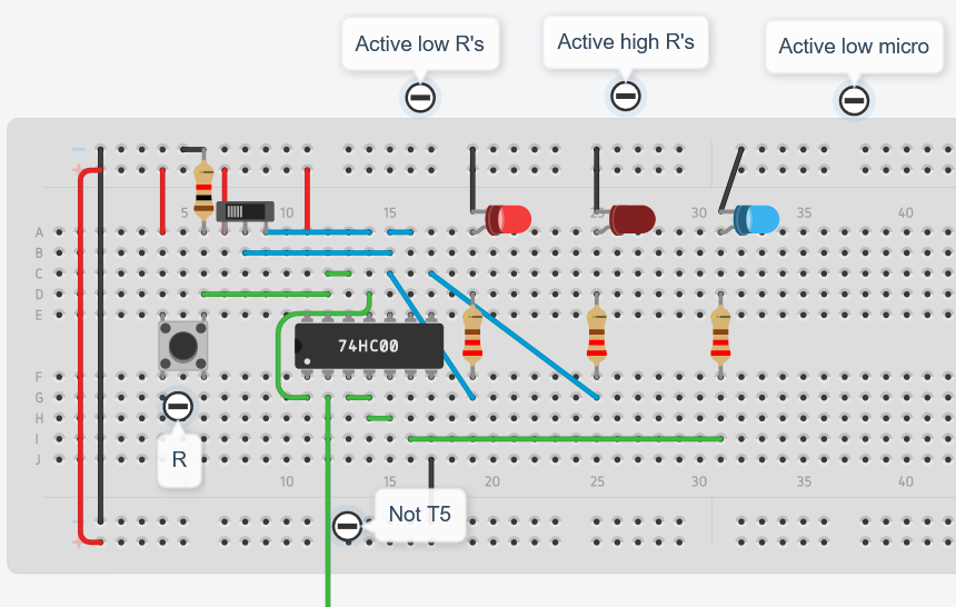
- Now connect the micro clock reset signal to the clear pin of the micro clock
- Connect the active high reset signal with active high clears:
- Instruction register
- Memory address register
- A register
- B register
- Connect the active low reset signal with active low clears:
- Program counter
- Output register
Schematic
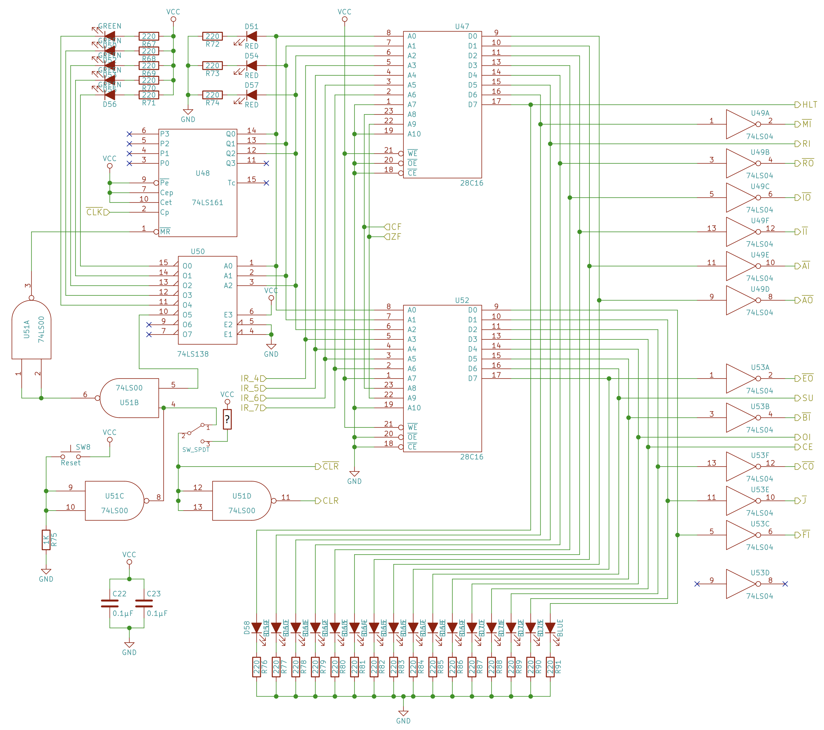
- As you can see I added the switch, and you may add a pull-up resistor instead of connecting directly to \(V_{cc}\). I’m using 330 Ohms.
- Although they appear in the schematic, I decided to not use LEDs for the microclock decoder as they do not provide any additional information compared to the 3 LEDs of the microclock
Last minute fixes
- Replaced the RC capacitor from 103 to 102
- Replaced the monostable pushbutton capacitor from 103 to 104
- Covered the 7-segment display with Babybel cheese red plastic wrappers…
- Replaced 250 ohm red LED resistors with 1k ohm resistors
- Add a 1k pull-down resistor to the left leg of the 102 capacitor in the RAM module to sink the decharging capacitor current and connect the clock pin of the other RAM chips directly to the system clock signal to avoid a potential double clock pulse in those chips.
- Found the bug that made the address register reset to 0. The “clear” signal fro m the R/C pushbutton is very weak and when the address register and ram have a large number of 0’s there seems to be too much noise/power difference or something that makes that triggers the clear pin as if it was floating and hence active high.
- Solution: disconnect the clear pin of the memory address register from the Reset/Clear signal (we don’t need to reset the address anyway as the fetch cycle will take care of loading the 0 address at the start of the program)
- To make the “runtime” inputs with HLTs work as expected make sure to hold the R/C button long enough to let the program counter value move to the memory address register, otherwise the micro clock would move to T1 before the address has been updated
- I’ve also removed the A and B register from the clear signal, it’s the responsibility of the programer to set those to 0 with code as the clear signal resetted those registers randomly
- Also did it for the flags register, the programmer must make a sum/subtraction before relying on the status of the flags register
- Replaced the 1k resistor in series with the potentiometer with two 10k resistors such that the maximum speed is bug free
Programs
- The programs below have been compiled to binary with this assembly compiler.
Adding two “runtime” inputs
- Differentiating HLT 15 as an input prompt unlike just HLT which would mean that the program ended:
address: contents    # assembly
---------------------------------
0000: 1111 1111      # 0.  HLT 15
0001: 0001 1111      # 1.  LDA 15
0010: 0100 1110      # 2.  STA 14
0011: 1111 1111      # 3.  HLT 15
0100: 0001 1111      # 4.  LDA 15
0101: 0010 1110      # 5.  ADD 14
0110: 1110 0000      # 6.  OUT
0111: 0110 0000      # 7.  JMP 0
1000: 0000 0000      # 8.  0
1001: 0000 0000      # 9.  0
1010: 0000 0000      # 10. 0
1011: 0000 0000      # 11. 0
1100: 0000 0000      # 12. 0
1101: 0000 0000      # 13. 0
1110: 0000 0000      # 14. 0
1111: 0000 0000      # 15. 0 //inputs
Incrementing counter
- Starts counting by 1 up to 255, then by 2 up to 255, then by 3 up to 255…
LDI 0 //start at 0 after overflow
OUT

ADD 15 //A += i
JPC 5 //loop while < 256 (CHECK BEFORE OUTPUTTING)

JMP 1 //loop while < 256

LDA 15
ADD 14
STA 15 // i is now (i+1)
JMP 0 // restart with new i
.
.
.
.
.
1 //increase of the increase
1 //intial increase i
address: contents    # assembly
---------------------------------
0000: 0101 0000      # 0.  LDI 0
0001: 1110 0000      # 1.  OUT
0010: 0010 1111      # 2.  ADD 15
0011: 0111 0101      # 3.  JPC 5
0100: 0110 0001      # 4.  JMP 1
0101: 0001 1111      # 5.  LDA 15
0110: 0010 1110      # 6.  ADD 14
0111: 0100 1111      # 7.  STA 15
1000: 0110 0000      # 8.  JMP 0
1001: 0000 0000      # 9.  0
1010: 0000 0000      # 10. 0
1011: 0000 0000      # 11. 0
1100: 0000 0000      # 12. 0
1101: 0000 0000      # 13. 0
1110: 0000 0001      # 14. 1
1111: 0000 0001      # 15. 1
Fibonacci sequence
- The strategy is to use 3 memory locations: 1111 for the last value, 1110 for the second last value, and 1101 as a temporary location to jiggle
- The code below starts initalizing the last value only (with 1), and it does not initialize the second last value outside of the loop as we would run out of lines so instead we just load A immedieately with 0.
- The idea is to have A at the end of each loop to contain the second last value and to output it at the beginning of the next loop
- Right after outputting A we add the 2 last numbers and do start jiggling the 3 memmory locations as defined by the code below.
LDI 1   # part 1 of ressetting the program to start with last number 1 and second last number 0
STA 15  # part 2 of resseting program
LDI 0   # part 3 of resseting the program, STA 14 can be skipped as we already have it in A register and it will be overwritten anyway

OUT     # should display second last number (order: 0, 1, 2, 3, 5, 8, 13, 21, 34. 55. 89, 144, 233)

ADD 15  # now we have A += last number

JPC 0   # moved it here for 2 reasons, after the out to not skip the 233 number and after the ADD to let the Carry flag get updated after overflowing (otherwise it will loop to 0 every time after overflowing once)

STA 13  # store the updated last number in temp location
LDA 15  # part 1 of moving previous last number to second last number location
STA 14  # part 2 of moving previous last number to second last number location
LDA 13  # part 1 of moving the new last number to the proper last number location
STA 15  # part 2 of moving the new last number to the proper last number location
LDA 14  # store A with second last number
JMP 3   # jump to output second last number

0    # temp value
0    # second last number
1    # last number
address: contents    # assembly
---------------------------------
0000: 0101 0001      # 0.  LDI 1
0001: 0100 1111      # 1.  STA 15
0010: 0101 0000      # 2.  LDI 0
0011: 1110 0000      # 3.  OUT
0100: 0010 1111      # 4.  ADD 15
0101: 0111 0000      # 5.  JPC 0
0110: 0100 1101      # 6.  STA 13
0111: 0001 1111      # 7.  LDA 15
1000: 0100 1110      # 8.  STA 14
1001: 0001 1101      # 9.  LDA 13
1010: 0100 1111      # 10. STA 15
1011: 0001 1110      # 11. LDA 14
1100: 0110 0011      # 12. JMP 3
1101: 0000 0000      # 13. 0
1110: 0000 0000      # 14. 0
1111: 0000 0001      # 15. 1
Multiplication of two integers
- The strategy is to bring the code below to assembly. See that i used a do while loop with a != 0 condition as it mostly approximates what we can do in assembly (we can’t do a normal loop with the condition being evaluated in the beginning since we first need to have an ALU operation to sets the flags in).
- If b is zero it will still run the loop once and then b becomes 11111111… if it’s negative it’ll start with a bunch of leading ones as well, taking a long time to bring b back to 0 (less time the bigger the negative number as it’s closer to 0 in 2’s complement)
- Funny enough, it takes 256 decrements to make b 0 again, which means that we would get \(result = 256 * A = 0 * A\) (doing the same addition 256 times results in A overflows that cancel each other out)
- For negative numbers we get \(result = a(256-b) = 256a - ab = -ab\)
- Although we do get the desired result, we do iterate (256-b) times
- Therefore, althgouh the program supports 0 and negative numbers for the “b” operand it is still advaisable to only use positive integers for b
Scanner input = new Scanner(System.in);

byte result = 0;
byte a = (byte) input.nextInt(); //5
byte b = (byte) input.nextInt(); //3

//int count = 0;
do {
    result += a; //5 + 5 + 5
    b--; //2, 1, 0
    //count++;
} while (b != 0);

System.out.println(result);
//System.out.println(count);
LDA 13
ADD 14
STA 13	//result += a

LDA 15
SUB 12
STA 15	//b--

JPZ 8  	// skip loop
JMP 0	// loop

LDA 13
OUT	// output result
HLT

. //junk

1 # b's decrement
0 # should be resetted to 0 each time
7 # a
3 # b
- You need to also set address 13 to 0 each time
address: contents    # assembly
---------------------------------
0000: 0001 1101      # 0.  LDA 13
0001: 0010 1110      # 1.  ADD 14
0010: 0100 1101      # 2.  STA 13
0011: 0001 1111      # 3.  LDA 15
0100: 0011 1100      # 4.  SUB 12
0101: 0100 1111      # 5.  STA 15
0110: 1000 1000      # 6.  JPZ 8
0111: 0110 0000      # 7.  JMP 0
1000: 0001 1101      # 8.  LDA 13
1001: 1110 0000      # 9.  OUT
1010: 1111 0000      # 10. HLT
1011: 0000 0000      # 11. 0
1100: 0000 0001      # 12. 1
1101: 0000 0000      # 13. 0
1110: 0000 0111      # 14. 7
1111: 0000 0011      # 15. 3