Arduino EEPROM programmer
Table of Contents
- Table of Contents
Pre-requisites
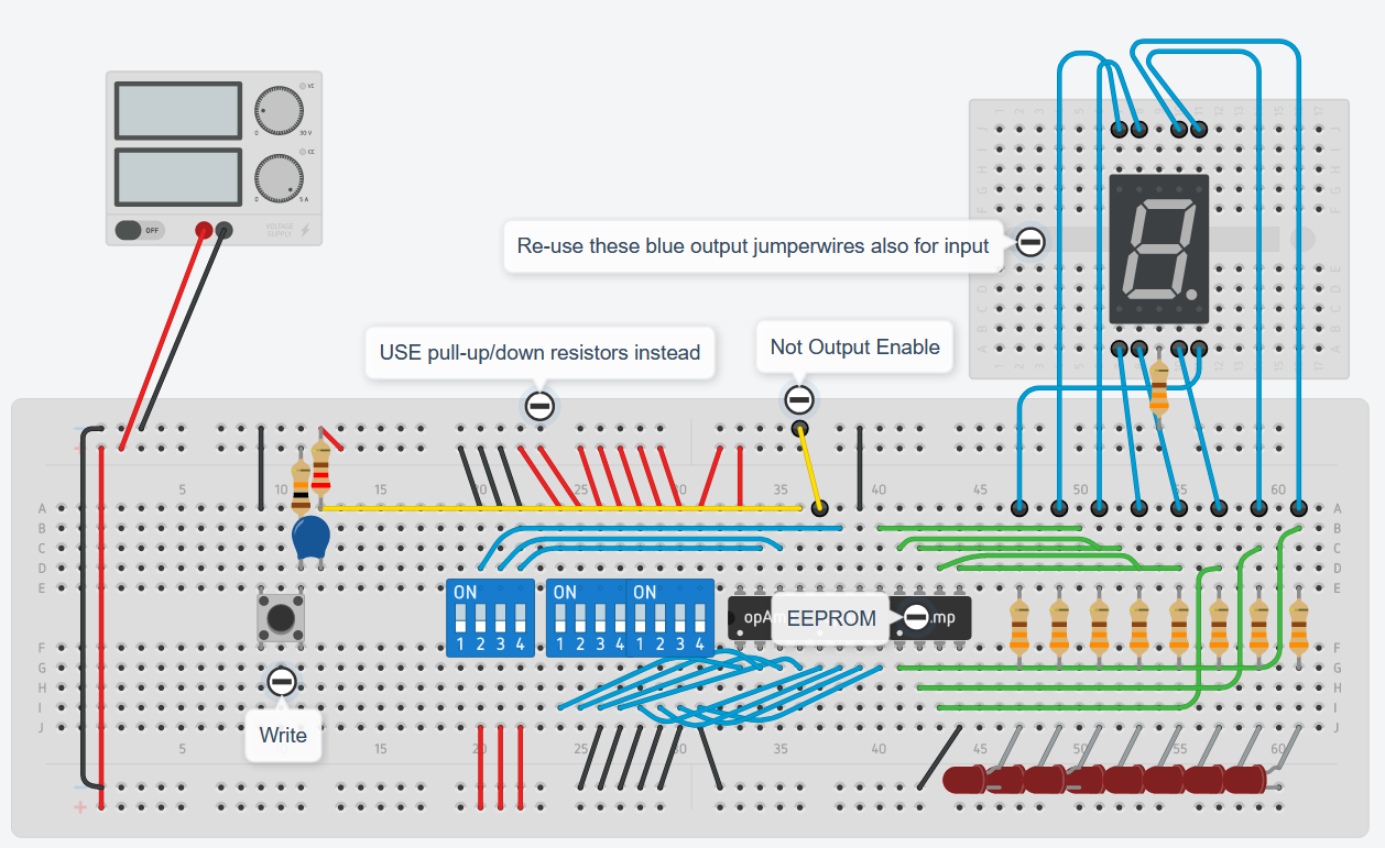
- You’ll need to have a way to debug the EEPROM, such as the program/debug breadboard circuit of the Ben Eater 8-bit computer project
- You’ll also need to be familiar with bitwise operations and object oriented programming. For a refresher you can check CSE1100 (Objected oriented programming (in Java)).
Arduino nano setup
- The goal is to automatically set the address, data, write enable/output enable pins for each write operation
- We’re gonna use the arduino nano, although the arduino uno could be used as well.
- The tinkercad implementation will be with arduino uno as nano is not available there.
- nano has the same functionalities but in a smaller form and it’s more compact
- It can be plugged directly into the breadboard and it comes with a USB port that can be connected to the computer to power up the microcontroller.
- Nano provides 5V and ground pins, so we can use them to power up the rest of the breadboard!
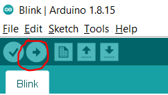
- To check if the microcontroller is working properly you can verify and upload the following code from Arduino’s IDE into the nano:
void setup() {
  // initialize digital pin LED_BUILTIN as an output.
  pinMode(LED_BUILTIN, OUTPUT);
}

// the loop function runs over and over again forever
void loop() {
  digitalWrite(LED_BUILTIN, HIGH);
  delay(1000);
  digitalWrite(LED_BUILTIN, LOW);
  delay(1000);
}
Windows 10 USB driver
- Tip: Double check the microcontroller that you bought. Ben’s kit came up with a CH340 nano, not an Arduino nano, therefore the USB drivers that came with Arduino’s IDE did not work. I had to install the drivers for CH340 Nano manually. Below what you could do with windows 10 and CH340 Nano:
- Download the Driver v3.4 (2016-09-27)
- Install Arduino 1.8.15
- Re-start the laptop
- Turn off Bluetooth
- Select the only port available (COM6 for the CH340 Nano)
- Under “Tools” select Arduino Nano as the “Board”
- Under “Tools” select ATmega328P (Old bootloader) as the processor
- Keep AVRISP mkll as the programmer
- Upload first the bare minimum example and then Blink from (File > Examples > Basics > Blink)
Digital pins
- Nano comes with the 12 data pins we can control while using the USB interface:
- D2
- D3
- D4
- D5
- D6
- D7
- D8
- D9
- D10
- D11
- D12
- D13
- RXO and TX1 cannot be used with the USB serial interface.
- We need to use the USB interface not only to power the circuit but also to be able to read the EEPROM and display it on our laptop/pc.
- However we have a total of 21 EEPROM pins we need to configure:
- 11 address pins
- 8 data pins
- Write enable
- Output enable
Shift register
- We can control many signals with just a few pins by using shift registers
- A shift register is essentially a combination of D flip-flops in series where the input of \(D_n\) is the output of \(D_{n-1}\) (Big Endian).
- At each clock pulse the data bits are shifted one position to the right.
- Because the shift register has just a single input (and the clock) but as many outputs as you want it’s very useful for scenarios where a microcontroller has less output pins that you need.
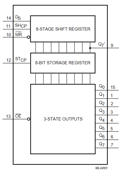
74HC595 (8-bit shift register)

- DS = data serial input
- SH_CP = shift clock pulse
8-bit Storage register
- The 74HC595 comes with an internal register that stores the contents between the shift register and the output pins
- Pin 12 (ST_CP) is the storage clock pulse.
- Behaves like an output “update” (rather than enable) signal. It is active high.
Testing Arduino and two 8-bit shift registers
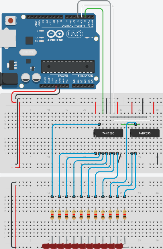
- Insert the arduino nano on the breadboard
- Connect 5V and GND pins to the power rails
- Insert 2 74HC595 8-bit shift registers
- Hookup power and ground pins
- Tie \(\overline{MR}\) (master reset) high
- Tie \(\overline{OE}\) low
- Comming from the arduino we’ll have:
- D2 of nano <-> DS (serial data) of left 74HC595
#define SHIFT_data 2
- D3 of nano <-> SH_CP (Shift register clock) of left and right 74HC595
#define SHIFT_CLK 3
- D4 of nano <-> ST_CP (storage rester clock) of left and right 74HC595
#define SHIFT_CLK 4
- These
#define constant nwith \(n\) as a number from 2 to 13 snippets is the way to define a constant in arduino code for the data pin n of the arduino board.
- D2 of nano <-> DS (serial data) of left 74HC595
- Hookup the Q7’ pin (serial data output, aka LSB Big Endian) of the left 8-bit shift register with the right one DS (serial data) input
- Hookup 11 MSB output pins to LEDs with resistors in series
- Upload the code below to the nano with the steps described at Arduino nano setup
- What we want to do is to set D2 (data input) with a specific value and alternate D3 (clock signal) high and low at a certain rate
- We could either manually program high and low bits for a pulse with a for loop, and set output high/low data pins in binary at the same rate, or use a built-in function that does it for us, (outputting and clocking) namely shiftOut() shifts out a byte of data one bit at a time.
shiftOut(dataPin, clockPin, bitOrder, value)- (int)
dataPin: the pin on which to output each bit i.e.SHIFT_DATA - (int)
clockPin: the pin to toggle once the dataPin has been set to the correct value. bitOrder: which order to shift out bits; eitherMSBFIRSTorLSBFIRT.- Since the value is a byte, whichever value you use between 0 and 255 will be turned into binary and padded with 0s such that you have 8 digits. LSBFIRT will display it in little endian (aka normal) and MSBFIRST the other way around.
- (byte)
valuethe data to shift out * We still need to manually trigger the storage/output clock to see the results.digitalWrite(pin, HIGH/LOW)function does it for us. - going from low, to high, to low should do the trick.
//Constants
#define SHIFT_DATA 2
#define SHIFT_CLK 3
#define SHIFT_LATCH 4

//Run only once
void setup(){
  //Set our constants (D2, D3 and D4) as output pins
  pinMode(SHIFT_DATA, OUTPUT);
  pinMode(SHIFT_CLK, OUTPUT);
  pinMode(SHIFT_LATCH, OUTPUT);

  //Shift LSBFIRST (output is displayed the same you write here)
  // LS shift register also comes first
  // Reminder that we only use it's 3 MSB bits,
  // shiftOut works at byte level
  // To output all 1's we just need:
  shiftOut(SHIFT_DATA, SHIFT_CLK, LSBFIRST, 0b11100000);
  shiftOut(SHIFT_DATA, SHIFT_CLK, LSBFIRST, 0b11111111);


//Trigger a clock pulse for the output clock signal
  digitalWrite(SHIFT_LATCH, LOW);
  digitalWrite(SHIFT_LATCH, HIGH);
  digitalWrite(SHIFT_LATCH, LOW);
}

void loop() {

}
- Think of OUTPUT/INPUT as the value of the DIR pin of the tri-state buffers that we had for the registers.
- We will have some sort of “BUS” between the 8-bit shift registers (controlled by the nano) and the EEPROM I/O pins.
- We only want to have 1 party outputting to the the BUS (aka driving), so output enable of EEPROM has to be turned off before we run
void setup()with all thepinMode(pin_n, OUTPUT). - If one of them (arduino or EEPROM) is trying to drive a zero on a particular bit and the other is trying to drive a one then you will effectively have a short from the positive power rail, through the output driver of (say) the EEPROM onto the bus and then down through the output driver of the Arduino to the ground rail.
- The output impedance of the devices can be quite low and so quite a large current can flow, this can cause the output drivers of both devices to be damaged.
- In the program this would only happen for a very short time (nanoseconds) and so the devices probably would be ok as there wouldn’t be time for heat to build up, but if, for example, you were single stepping through the code, it could be in that state for quite some time and damage could easily occur. Best practise is to ensure there is only one device driving the bus at any one time.
- For now we don’t have a BUS, just LEDs with resistors.
Tinkercad
EEPROM Address
- Once the implementation of storing 11 bits into the shift registers has worked, we can refactor the
setup()code regarding the storage off 11 bits intosetAddress(int address)and the output clock pulse into, which is used to latch the shift register content into the shift register output pins, aslatch().- Luckily arduino comes with function
digitalRead(pin_number)that returns the value of that pin. We can use it to subtly toggle the clock, and later to read EEPROM data.
- Luckily arduino comes with function
/**
* Triggers a clock pulse for the shift register output clock signal
*/
void latch(){
  digitalWrite(SHIFT_LATCH, !digitalRead(SHIFT_LATCH));
  digitalWrite(SHIFT_LATCH, !digitalRead(SHIFT_LATCH));
}

/**
* Sets the address in little endian by splitting it into right and left register
*/
void setAddress(int address) {
  int rightRegister = address & 0b00000000111;
  int leftRegister = address & 0b11111111000;
  shiftOut(SHIFT_DATA, SHIFT_CLK, LSBFIRST, rightRegister << 5); //3 LSB significant bits padded with 5 zeros to the right
  shiftOut(SHIFT_DATA, SHIFT_CLK, LSBFIRST, leftRegister >> 3); //8 most significant bits (of an 11bit address)
  latch();
}
- Since the shift register is only used by the setAddress method, you may as well keep
latch()functionality withinthe setAddress()method. - Ben Eater address implementation uses the most significant LED to store the least significant bit. That’s what I’ve been calling “Big Endian” so far in the 8-bit computer project.
- Although its display is inverted (if you input address
0b00000000001, you’d see lighting up the leds in the fashion10000000000, it’s address method implementation is much cleaner and the bits actually line up with the outpin numbers of the 8-bit shift register datasheet:
void setAddress(int address) {
  shiftOut(SHIFT_DATA, SHIFT_CLK, MSBFIRST, address >> 8);
  shiftOut(SHIFT_DATA, SHIFT_CLK, MSBFIRST, address);

  //Triggers a clock pulse for the shift register output clock signal
  digitalWrite(SHIFT_LATCH, !digitalRead(SHIFT_LATCH));
  digitalWrite(SHIFT_LATCH, !digitalRead(SHIFT_LATCH));
}
- We’re going to go with Ben’s style as it will probably fit better with the breadboard pin layout he has prepared.
- On top of this, Ben also wants to use the LSB (in terms of leds, but rather the 8th output pin) of the “register on the left” as the signal for \(\overline{OE}\) of the EEPROM.
- For that we will bitwise sum the data input for the first shiftOut (the one that’ll end up on the register on the left) with either a 1 or a 0 in the binary most signicant position such that it ends up in the 8th output pin of the second register, since it’s active low, we sum 0 if it’s
trueand 128 (0b10000000, which ends up with the 1 at 0b00000001, that is the 8th output pin) if it’sfalse.
- For that we will bitwise sum the data input for the first shiftOut (the one that’ll end up on the register on the left) with either a 1 or a 0 in the binary most signicant position such that it ends up in the 8th output pin of the second register, since it’s active low, we sum 0 if it’s
/**
 * Sets the address and output enable
 */
void setAddress(int address, bool outputEnable) {
  shiftOut(SHIFT_DATA, SHIFT_CLK, MSBFIRST, (address >> 8) | (outputEnable ? 0 : 128));
  shiftOut(SHIFT_DATA, SHIFT_CLK, MSBFIRST, address);

  //Triggers a clock pulse for the shift register output clock signal
  digitalWrite(SHIFT_LATCH, !digitalRead(SHIFT_LATCH));
  digitalWrite(SHIFT_LATCH, !digitalRead(SHIFT_LATCH));
}
- Indeed, now that we can proceed to move from the test LEDs to outputting the output pins of the shift registers into the EEPROM address pins, we see that Ben connects what was before the “Left most” LED, which with the second shiftOUt (
shiftOut(SHIFT_DATA, SHIFT_CLK, MSBFIRST,address)) ended up with the least significant bit is connected to the least significant EEPROM address pin (A0) - Therefore, connect the EEPROM, it’s power and ground pins, chip enable to ground, and connect the shifht register outputs into the EEPROM pins in the same fashion.
- Use the 8th output of the right register to connect it to output enable
EEPROM data I/O
- The only thing that is left to connect to the EEPROM are the I/O pins (8) and write enable, for which we have D5 to D13 of the arduino nano!
- D5 = I/O 0
- D6 = I/O 1
- …
- D12 = I/O 7
- D13 = \(\overline{WE}\)
Tinkercad
- The final breadboard layout should look like this:
Open tinkercad
Reading the EEPROM
- Steps:
- Free up the BUS
- Set load the address and enable EEPROM output
- Read I/O pins via D5-D12
- Feed it to the USB (we can because we’re not using the 2 first data pins of the nano)
- Optional: improve the format of the monitor by using a foor loop and displaying each byte as a two digit hex number in a 16 x 16 matrix (that displays a total of 256 bytes)
#define EEPROM_D0 5
#define EEPROM_D7 12
...
/**
 * Read a byte from the EEPROM at the specified address.
 */
byte readEEPROM(int address){
  /* Since we need the EEPROM to output to the "I/O BUS", we need to make sure that at most 1 party is outputting at a time */

  // Set arduino Data pins to be input (thus freeing the BUS)
  for (int pin = EEPROM_D0; pin <= EEPROM_D7; pin++) {
    pinMode(pin, INPUT);
  }

  //Load address into the EEPROM, and output enable EEPROM (the boolean)
  setAddress(address, true);

  byte data = 0; //initialize byte

  //Populate byte with the I/O BUS contents
  //start reading MSB first, then shift data to the left each time before summing next pin
  for (int pin = EEPROM_D7; pin >= EEPROM_D0; pin--) {
    data = (data << 1) + digitalRead(pin);
  }

  return data;

}
Serial.begin(speed)opens the USB Serial port and sends that many bits at that rate per seconds via pins 0 and 1.void setup(){ ... Serial.begin(4800) ; //opens USB port and sends that many bits at that rate per seconds Serial.println(readEEPROM(0)); //print at arduino IDE! }- Go to “Tools” > “Serial Monitor” and then upload the program to the nano to see the results
- Make sure that the baud speed of the Serial Monitor is the same as the Serial.begin()
- The optional display in hexadecimal for 256 addresses:
/*
 * Read the contents of the EEPROM and print them to the serial monitor.
 */
void printContents() {
  for (int base = 0; base <= 255; base += 16) {
    byte data[16];
    for (int offset = 0; offset <= 15; offset++) {
      data[offset] = readEEPROM(base + offset);
    }

    char buf[80];
    sprintf(buf, "%03x:  %02x %02x %02x %02x %02x %02x %02x %02x   %02x %02x %02x %02x %02x %02x %02x %02x",
            base, data[0], data[1], data[2], data[3], data[4], data[5], data[6], data[7],
            data[8], data[9], data[10], data[11], data[12], data[13], data[14], data[15]);

    Serial.println(buf);
  }
}
Writting the EEPROM
- Steps:
- Define write enable pin at the top of the code:
#define WRITE_ENABLE 13 - Set the Address and disable the EEPROM from using the BUS and making it’s I/O pins
- Set D5-D12 as output pins
- Start the \(\overline{WE}\) pin high to comply with the datasheet timing, and that it’s an output pin of the arduino.

void setup(){...digitalWrite(WRITE_ENABLE); pinMode(WRITE_ENABLE, OUTPUT);...}- Load each data pin in the BUS with it’s corresponding high or low signal.
- Toggle the \(\overline{WE}\) pin low, delay between 100ns and 1000ns (1 microsecond) to trigger the write operation.
- Delay/Poll for next write cycle:
- Although the Write Cycle Time is spec’d as max 1ms, you really shouldn’t just assume a 1ms delay will do the trick. If you wanna read immideately after writting, you’ll see that the MSB bit has an inverted value (and the remaining bits are “indetermined”) until the EEPROM is done writting the data. The correct implementation would be to perform a read loop after a write, to check for a non inverted MSB of the byte just written, which then confirms that writing is completed. This is known as data polling and it is indeed a feature of the AT28C16 EEPROM that we use.
- Or you can do a poorman’s implementation and add an ad-hoc delay (
delay(10)) to increase the Write Cycle Time.
- Or you can do a poorman’s implementation and add an ad-hoc delay (
- Although the Write Cycle Time is spec’d as max 1ms, you really shouldn’t just assume a 1ms delay will do the trick. If you wanna read immideately after writting, you’ll see that the MSB bit has an inverted value (and the remaining bits are “indetermined”) until the EEPROM is done writting the data. The correct implementation would be to perform a read loop after a write, to check for a non inverted MSB of the byte just written, which then confirms that writing is completed. This is known as data polling and it is indeed a feature of the AT28C16 EEPROM that we use.
- Define write enable pin at the top of the code:
/*
 * One Write cycle of a byte into the EEPROM at the specified address.
 */
void writeEEPROM(int address, byte data) {
  //Not only set addres, but also disable EEPROM from driving the BUS (and setting it's I/O pins as I)
    setAddress(address, /*outputEnable*/ false);

    //Setting our D5 to D12 pins (their names offseted to start at D0) as outputs
    for (int pin = EEPROM_D0; pin <= EEPROM_D7; pin++) {
        pinMode(pin, OUTPUT);
    }

    // keep track of msb for polling write completion
    byte msb = data & 128;

    // write our byte starting from the least significant bit, (then shifting the given data to be written once to the right such that next least significant bits are the ones stored
    for (int pin = EEPROM_D0; pin <= EEPROM_D7; pin++) {
        digitalWrite(pin, data & 1); //writes LSB bit
        data = data >> 1;
    }

    // toggle write enable pin
    digitalWrite(WRITE_ENABLE, LOW);
    delayMicroseconds(1); //right at the maximum write pulse width value because arduino cant go lower
    digitalWrite(WRITE_ENABLE, HIGH);

    // at this point a write should be in progress...
    //delay(10); arbitrary delay


    byte pollBusy = readEEPROM(address) & 128;
    while (pollBusy != msb) {
        delay(1);
        pollBusy = readEEPROM(address) & 128;
    }
}
Delete all
/**
 * Erases entire EEPROM with 0xff
 */
void deleteAll(){
  Serial.print("Erasing EEPROM");
  for (int address = 0; address <= 2047; address++) {
    writeEEPROM(address, 0xff);

    if (address % 64 == 0) {
      Serial.print(".");
    }
  }
  Serial.println(" done");
}
Programm data bytes
- We’ll program a 4-bit hex decoder for a common cathode 7-segment display by storing it in a byte data array.
- Then we can use that data into the method below:
byte data[] = { 0x7e, 0x30, 0x6d, 0x79, 0x33, 0x5b, 0x5f, 0x70, 0x7f, 0x7b, 0x77, 0x1f, 0x4e, 0x3d, 0x4f, 0x47 };
/**
 * Program data bytes
 */
void program(){
  Serial.print("Programming EEPROM");
  for (int address = 0; address < sizeof(data); address += 1) {
    writeEEPROM(address, data[address]);

    if (address % 64 == 0) {
      Serial.print(".");
    }
  }
  Serial.println(" done");
}
- Ben Eater programmed the data array in such a way that ‘a’ segment is at the 7th bit, ‘b’ at the 6th, etc and the dot, is the 8th bit, the one that I damaged probably with data polling, fortunately it is left unused for the 7-segment decimal display.
Repository
- You can check the forked repository with the suggested changes here: https://github.com/skirienkopanea/eeprom-programmer


